In this article, we introduced the inner layer processing in the PCB manufacturing process, and then we will introduce the outer layer processing process.
Step 9: Drilling
Once the stackup is pressed and cured, the stack is ready for drilling and plating. A CNC drill is used to place drill holes in the stack by following the information in your NC drill files. The drill data that was prepared at the end of the design phase is used to program and tool these machines.
Step 10: Deburr, Desmear, and Copper Deposition
After drilling, any formed holes are prepared for plating using a deburr process (to smooth out hole edges) and desmear process (to smooth resin along the hole wall). Finally, the holes and visible surface are plated with an electroless copper deposition process. This process involves an electrolytic chemical reaction with a solution containing copper ions, and a thin copper film will naturally deposit along the walls of drilled holes and the visible surfaces. This leaves behind a seed layer that will be coated with additional copper in Step 12.

Step 11: Coat With Photoresist and Expose
A dry (non-liquid) photoresist material is used to coat the plated copper on the outer layers. This photoresist is also exposed in the same manner as in Step 3, except the stencil is now a positive image that matches the hole and trace pattern that will appear on the top layer. The remaining un-exposed photoresist is removed with a solvent.

Step 12: Electroplating
After photoresist exposure, the visible copper on the surface layers is plated with additional copper using an electroplating process. This is an electrochemical process that involves running an electric current through a plating solution to drive copper deposition. This continues until the copper on the exposed layers is plated to the desired weight.

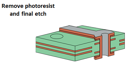
Step 13: Photoresist Strip and Etch
The remaining photoresist is stripped with a solvent, and the leftover electroless copper seed layer from Step 11 is etched with an etching solution. This is the final step involving copper deposition and etching, and it leaves behind finished traces and plated holes.
Step 14: Solder Mask Application
In this step, the solder mask is applied to provide a protective layer for copper features on the surface layer. There are three main types of solder mask materials:
- Liquid epoxy: This solder mask material is screen printed through a stencil. This solder mask material and its application process is best used when required solder mask openings are relatively large. Most manufacturers will use a photoimageable material as smaller feature sizes can be formed.
- Liquid photo-imageable (LPI): This material is applied uniformly to the surface layer and exposed to UV light through a negative stencil image. The exposed areas will harden, while the remaining unexposed material is removed with a solvent.
- Dry film photo-imageable: This solder mask material is a dry film that is applied as a sheet and vacuum-sealed onto the surface layer. The film is then exposed and removed in the same process as LPI.
Step 15: Surface Finish and Silkscreen Printing
Surface finishes are applied in this step. These finishes apply a top plating layer to any copper exposed through the solder mask to provide additional environmental protection and surface for soldering. You can read more about surface finishes in Lesson 5 in this unit. The final fabrication step is printing silkscreen on top of the solder mask.