FAQs
PCB & PCBA
Frequently Asked Questions
Table of Content
Want Talk TO US?
Contact us
01.
General Questions
JHYPCB is your trusted, global professional supplier of electronic manufacturing services. We can provide turnkey services in all stages of PCB manufacturing, from prototype to mass production.
One-stop solutions include:
- PCB prototype service
- PCB fabrication service
- PCB assembly service
- Components sourcing service
- PCB & PCBA Testing service
Although we receive a lot of inquiries, in almost all cases, we will quote within one day of receiving the inquiry; usually, we expect a response within 4 hours.
We accept direct bank transfers, PayPal, Alipay, or credit card payments. For new customers we expect first order to be paid in full on placement of order. This allows to us begin the process of Credit Checks and Account Opening.
To learn more, see our payment options.
No, Even if you only need 1pcs, we provide the service you need.
Yes, we provide Free PCB prototypes, and the qty is no more than 5pcs. But we need to charge the prototypes first and return the PCB prototype cost in your mass production if your sample order value is not more than the mass production value’s 1%.
You will bear the VAT and Tariff. VAT and tariff vary in different countries of the destination. If products exporting to you, we can reduce and declare the invoice value as low as your requirement to save cost.
We respect our clients’ copyrights and will keep them strictly confidential.
Our hours of operation are as follows (China time zone):
- 9:00 a.m. – 18:00 p.m. (GMT+8) from Monday to Friday
- 9:00 a.m. – 12:00 a.m. (GMT+8) Saturdays.
- We do not work on Sundays and public holidays.
However, we provide 7*24 hours service. During the off-duty period, the production of our PCB factory and assembly factory will be uninterrupted, and we have staff on duty standing by to handle your needs.
PCB Manufacturing FAQs
Compared to standard plated-through-hole PCBs, the required technical equipment and additional procedures to manufacture these PCBs are more complex.
– multiple drilling procedures
– precise z-axis machines for blind vias
– horizontal electroplating for plating-through blind vias
JHYPCB’s engineering team will use every possibility to reduce costs for you. We provide PCB panelization services; of course, you can also provide us with panelization files.
Learn more about What is PCB Panelization and its Methods in PCB Manufacturing?.
The possibility of arranging several boards in one panel depends on their size. In principle, we recommend the fabrication in one panel when ordering several small boards. The size of a panel should not exceed 609 mm by 889 mm. Additional costs may occur if you require specific panel sizes.
A typical PCB thickness is 0.063 inches or 1.57mm, a standardized level defined in the past. This is because 0.063″ is the thickness of plywood boards used as substrates for electronic devices, including PCBs, in the plywood industry.
The minimum PCB thickness that JHYPCB can handle is 0.4mm.
If there is no change in the PCB manufacturing process, we will no longer charge the Tooling costs.
There are three types of machining in the PCB manufacturing process:
- Drilling
- V-cut/Scoring
- Routing
If the solder mask is applied in identical size to the copper pads, its clearances will not accurately fit due to fabrication tolerances and may partially cover the pads. This prevents flawless soldering of the PCBs.
The solder mask should therefore be 0.1 mm to 0.2 mm larger (surrounding the structure by 0.05 mm to 0.1 mm) than the copper pads. This applies to pads, fiducial marks, text, or logos. In general, it is recommended to enlarge the entire mask by a constant factor appropriate to these structures.
Yes, although green is our most common PCB color, JHYPCB can provide solder masks in various colors: green, black, white, red, blue, purple, etc.
At JHYPCB, we can provide the following surface finish processes:
- Hot Air Solder Level (HASL)
- Lead-Free HASL
- Organic Solderability Preservatives (OSP)
- Immersion Gold
- Immersion Silver
- Immersion Tin
- Electrolytic Hard Gold (Finger Gold)
- Electroless Nickel Electroless Palladium Immersion Gold (ENEPIG)
Solder mask bridges are necessary to separate adjacent rectangular pads. If these structures are carried out too thin, they are possibly less stable and may chip off the circuit board, thus preventing flawless soldering. This is particularly problematic concerning IC (integrated circuits), which have marginal pitches. Suppose the pitch between two pads measures 0.20 mm to 0.25 mm only. In that case, an entire application of soldering mask onto all pads without soldering mask bridges is recommended, as the minimum size of these would already be 0.1 mm plus the diameter of the pad.
However, please rest assured that at JHYPCB, we will arrange the production time of your order reasonably. Our salesman will negotiate the delivery time with you in advance, and do all the production preparation and delivery work.
We specialize in a wide range of PCB segments such as:
- single-sided PCBs,
- double-sided PCBs,
- multilayer PCBs,
- Rigid PCBs,
- Flexible PCBs,
- Rigid-flex PCBs.
Among them, multi-layer PCB and flexible PCB manufacturing services are our advantages.
We have capacities for manufacturing most custom PCBs, and we list our PCB manufacturing capacities for all kinds of PCBs we can fabricate on our website. If you don’t understand them, or if your PCB board requires special processing or you are not sure whether we have the capacities to fabricate, don’t hesitate to get in touch with us.
We only provide a quick quote through manual review, which can ensure the quote and lead time are accurate. The PCB quick quote can be sent in 12 hours. In the file reviewing the preparations includes
(1) Issuing Engineering Questions if have, any and solving them together with you.
(2) making working Gerber of your design.
(3) panelizing your design in a working set and panelizing your working set into a significant manufacturing panel with or without other design sets.
(4) making manufacturing instruction (MI).
(5) printing films of the circuitry of each copper layer, solder mask of each layer, silkscreen of each layer, and other preparations. Of course, some of these preparations have a time sequence, and others can be done simultaneously.
This is a time-costly process; our engineer will do DFM Check and may give feedback on whether the PCB design is manufacturable or whether our manufacturing capacities can manufacture this circuit board. But please send files with the format we support, PCB spec, and quantity together.
03.
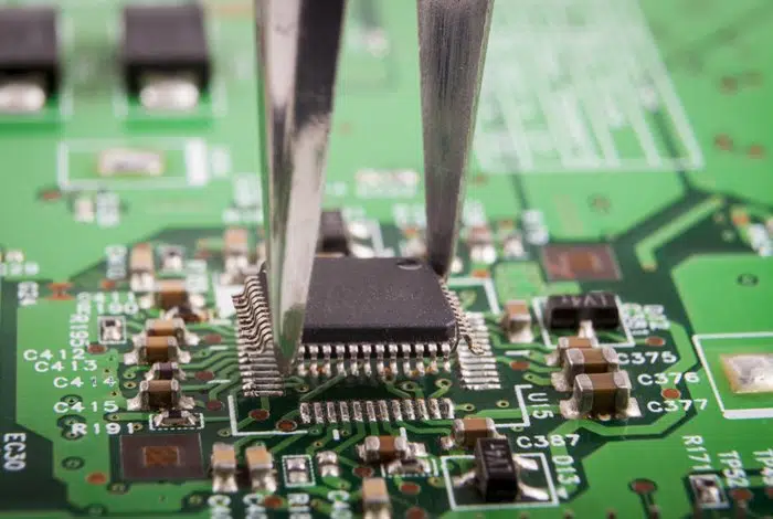
PCB Assembly FAQs
Yes. Whether you want to supply components yourself or want us to purchase components on your behalf, we provide assembly services. For details, you can refer to our consignment PCB assembly service and full turnkey PCB assembly service.
Yes, we offer turnkey PCB assembly service, including Printed Circuit Board Fabrication, All parts Sourcing, SMT Stencil, Assembly, and Testing.
For PCB assembly, we hope that you can provide the following information accurately:
- PCB Gerber
- Bill of Materials (BOM
- Pick & Place File
- Quantity Required
- Leadtime expected
- Assembly Drawing
- special requirements and instructions.
For more, see PCB Assembly Files.
Yes, we manufacture PCBs using Lead-Free Solder. In exceptional circumstances, Non-Rohs can also be offered.
Learn more our Lead-free PCB Assembly Service.
Yes, the advantage of getting PCB assembly service from China is that it can provide you with low-cost PCB assembly service with guaranteed quality.
What types of PCB assembly technology exist? JHYPCB utilizes surface mount technology (SMT) and through-hole technology (THT) to assemble PCBs. SMT involves “placement” components to a PCB, while through-hole uses wave soldering for unique products and prototypes. SMT is the preferred choice because components can be placed on either side.
Through-hole technology is best for mixed-technology PCBs. JHYPCB uses wave soldering RoHs, Non-RoHs, and conformal coating to build through-hole PCBs.
Centroid file is also called pick and place file. This data, including X, Y, rotation, side of board (to or bottom component side) and reference designator, can be read by the SMT or thru-hole assembly machines.
PCB assembly cost differs from PCB spec, parts type, total parts on a PCB, and order quantity. Please send us your Gerber files and BOM, and after the review by our engineer, the PCB assembly cost will be offered.
Related Reading:
We have capacities for assembling most PCBAs, and we list our PCB assembly capacities on our website. If you don’t understand them, or if your PCB assembly requires special processing, or you are unsure whether we can assemble your PCB boards, don’t hesitate to get in touch with us.
We count the lead time of the PCB assembly order from the date of placing an order to us and the payment receipt. Our quotation will include PCB manufacturing lead time, components sourcing lead time, assembly lead time, and whole estimated delivery time.
Generally, PCB manufacturing and components sourcing can be done simultaneously, but the lead time of component sourcing will be longer. Assembly turn-time begins immediately after the PCBs, all components are ready, and the information received is complete. For prototype PCB assembly, the assembly lead time is always 2-3 working days. For mass production, we can give an accurate delivery time when the result of the productivity and yield of the 1st shift comes out. Of course, we will inform you if there is any update on the progress.
Yes, We provide framed and frameless laser cutting PCB stencil fabrication services. For more SMT stencil making services please click here.
After receiving your loaded PCB assemblies, contact us immediately if you run into any problems. We will evaluate the issue and repair (rework) or remake as appropriate after determining the root cause of the problem.
PCB assembly according to IPC-A-610 Class II.
Fixtures and other objects include PCB E-test fixtures, Solder Paste Stencil, SMT Assembly Fixture (/ SMT support plate), IC programming fixture, PCBA testing fixture, PCBA testing fixture, PCB punching die (/mold), and parts remaining. We can keep them for free in suitable conditions for one year from the shipping date. But please remember that in such long stock, we cannot promise whether they are in good quality for your next repeat orders. If it happens broken, we will have no responsibility for making a new one.
Yes, We can handle BGA of 0.25mm pitch with X-ray testing. For BGAs, there are two designs via on pad and near pad connected by shorter trace. We need to tent and fill any vias near the pad of the BGAs with a solder mask to ensure the soldering quality. But for vias on the pad, we need to fill via with resin to ensure good soldering quality.
Click here to learn more about our BGA assembly services.
We occasionally encounter component loss and damage during the assembly process due to mis-insertion. Therefore for a smooth and uninterrupted assembly flow, we ask for a 3% for attrition purposes. All unused parts will be sent back with the assembled boards.
Yes, we will do detailed testing and inspection after the first batch of 5-10 pieces is assembled and send the final report and photos to you for confirmation. We will continue production only after your confirmation.