


PCB Assembly Services
PCB Assembly Process
Electronics play an essential role in our daily lives, powering everything from smartphones to cars. At JHYPCB, we understand the importance of quality printed circuit boards (PCBs) as the foundation of these electronic devices.
Most people recognize PCBs as the small green chips covered in lines and copper parts found in electronic devices. However, these boards are more than just decorative pieces. A PCB with components mounted on it is called an assembled PCB, and the manufacturing process is called PCB assembly (PCBA). The copper lines on the bare board, called traces, electrically link connectors and components to each other, allowing the circuit board to function in a specifically designed way.
JHYPCB provides a one-stop shop for PCB prototype, manufacturing, and assembly services. Our advanced assembly process consists of both manual and automated steps, ensuring high-quality and reliable PCBA. We work closely with our clients to provide customized solutions that meet their specific requirements, from BOM management to testing and inspection. With our expertise and dedication to quality, JHYPCB is the ideal partner for your PCB assembly needs.
Comprehensive PCB Assembly Services at JHYPCB
At JHYPCB, we offer comprehensive PCB assembly services to meet the needs of businesses and organizations across a wide range of industries. From initial design and prototyping to full-scale production, we are dedicated to providing our customers with high-quality, reliable PCB assemblies that meet their specific requirements. With state-of-the-art facilities and a team of experienced professionals, we are committed to delivering top-notch results on every project. In this article, we will take a closer look at the comprehensive PCB assembly services that we offer and the benefits that they provide to our customers.
JHYPCB provides a wide range of PCB assembly services, including:
Surface Mount Technology (SMT) assembly: This process involves the placement of surface mount components, such as resistors, capacitors, and integrated circuits, onto the PCB using automated pick-and-place machines.
Through-Hole Technology (THT) assembly: THT assembly involves the manual placement of through-hole components, such as connectors and switches, onto the PCB and soldering them in place.
Mixed Technology assembly: This process combines both SMT and THT assembly methods to accommodate both surface mount and through-hole components.
Single or Double-Sided PCB assembly: JHYPCB can assemble single or double-sided PCBs depending on customer requirements.
Full Turnkey assembly: We offer a full turnkey service, which includes PCB fabrication, component procurement, assembly, testing, and final packaging.
Partial Turnkey assembly: JHYPCB can also offer partial turnkey assembly services, where customers provide some components while we procure the rest and perform the assembly.
PCB prototype assembly: We offer PCB assembly services for prototypes, allowing customers to test their designs before moving on to mass production.
Box build assembly: JHYPCB can also provide box build assembly services, which involve the assembly of PCBs into a finished product enclosure.
With our advanced equipment and experienced team, JHYPCB can handle both small and large volume PCB assembly projects, providing high-quality and reliable solutions to our clients.
PCB Types JHYPCB Can Assemble
At JHYPCB, we specialize in providing a wide range of PCB assembly services to meet the unique needs of our customers. Whether you need a simple single-sided PCB or a complex multi-layered design, our team has the experience and expertise to handle even the most challenging projects. With our state-of-the-art facilities and advanced assembly equipment, we can assemble a wide variety of PCB types, including surface mount technology (SMT), through-hole technology (THT), and mixed technology boards. In this article, we will explore the various types of PCBs that JHYPCB can assemble and the advantages of each type.
JHYPCB can assemble various types of PCBs, including:
Rigid PCBs: These are the most common type of PCBs and consist of a solid, inflexible board material, such as fiberglass or FR-4.
Flexible PCBs: Also known as flex PCBs, these are made of a flexible material, such as polyimide, that can bend or twist without breaking.
Rigid-Flex PCBs: These combine the best of both rigid and flex PCBs, featuring both solid board sections and flexible sections in a single PCB.
High-Density Interconnect (HDI) PCBs: HDI PCBs are designed for high-density electronic applications and have smaller vias and trace widths, allowing for more components in a smaller space.
Metal Core PCBs: These PCBs have a metal core, usually aluminum, that acts as a heat sink and dissipates heat away from the components.
Ceramic PCBs: These are made from ceramic materials, providing high thermal conductivity, high insulation resistance, and excellent dimensional stability.
JHYPCB has extensive experience in assembling all of these PCB types, ensuring the highest quality and reliability for our customers.
What is the PCB Assembly Process?
Now in this era, electronic devices are an essential part of our daily lives. Everything from our mobile phones to our vehicles includes electronic components. At the guts of those electronics is the printed circuit board, also called a PCB. The general public recognizes printed circuit boards once they see them. These are the little green chips covered in lines and copper parts you will find in the guts of gutted electronic devices. A PCB with components mounted on is termed an assembled PCB and also the manufacturing process is named PCB assembly or PCBA for brief. The copper lines on bare board, called traces, electrically link connectors and components to every other. They run signals between these features, allowing the circuit board to function in an exceedingly specifically designed way. These functions range from the straightforward to the complex, and yet the dimensions of PCBs are often smaller than a thumbnail.
Terminology for PCB assembly
Surface Mount Technology: A technique for directly mounting electronic components onto a printed circuit board.
Through-hole Technology: A technique for inserting components into a printed circuit board through holes.
Pick and Place (P&P): An automated equipment used to pick up electronic components from a component library and place them onto designated positions on a printed circuit board.
Reflow soldering: A technique for soldering electronic components onto a printed circuit board using high-temperature hot air or infrared heating to melt the solder and create a connection between the components and the board.
Wave soldering: A technique for soldering electronic components onto a printed circuit board by passing the board through a wave of molten solder, which attaches the solder to the component pins and pads on the board.
Bill of Materials (BOM): A list that outlines all the components and materials needed to manufacture a PCB assembly.
Assembly Drawing: A drawing that shows the position and orientation of each electronic component on the printed circuit board, typically used in conjunction with the BOM.
X-Ray Inspection: A method of using X-rays to inspect the installation and soldering of components on a printed circuit board to ensure quality and reliability.
In-Circuit Test (ICT): A test conducted after electronic components have been soldered onto a printed circuit board to check for correctness, connectivity, and electrical performance.
Functional Test (FT): A test conducted after a printed circuit board assembly has been completed to ensure that the board’s function and performance meet specifications.
Design for Manufacturing (DFM): Designing a printed circuit board with consideration for manufacturing and assembly factors to ensure ease of manufacture and assembly, minimize costs, and improve production efficiency.
Design for Testability (DFT): Designing a printed circuit board with consideration for testing and diagnosis factors so that the board can be tested and diagnosed easily and quickly after manufacture and assembly.
Lead-Free (LF) Assembly: Using lead-free solder to assemble a printed circuit board to meet environmental and health requirements.
Ball Grid Array (BGA): A form of electronic component packaging in which the pins are arranged in a grid of balls that connect to solder on the printed circuit board.
Quad Flat Package (QFP): A form of electronic component packaging in which the pins are arranged in a rectangular pattern that connect to pads on the printed circuit board.
Surface Mount Device (SMD): An electronic component that is directly mounted onto a printed circuit board using SMT technology.
Component Footprint: The space and connection method used by an electronic component on a printed circuit board.
Silkscreen: A layer on a printed circuit board used to display component position, pin marking, board identification, and other information.
Panelization: Arranging multiple printed circuit boards onto a larger panel for manufacturing to improve efficiency and reduce manufacturing costs.
Gerber File: An electronic file format used to describe the graphics and text information required for the manufacture of a printed circuit board.
Information and Documents Required for PCB Assembly
The information and documents that customers need to provide for PCB assembly may vary depending on the specific production requirements and customer needs, but here are some common ones:
Gerber files: Gerber files contain the image data of each layer of the circuit board, including the circuit diagram, holes, surface mount and through-hole pads, etc. This is the basic data required for PCB production.
Circuit board design: The circuit board design is essential design data for PCB production. The design includes the circuit diagram, component layout, pads, and surface mount components.
Bill of materials: The BOM lists all the components and materials required for the circuit board, including the brand, model, quantity, and packaging form of the components.
Solder mask: The solder mask is a covering material that protects the non-soldering area of the circuit board. The solder mask should include a file with the location of pads and surface mount components.
Specifications: The specifications provide detailed information on the requirements and standards for the circuit board, including the board size, appearance, quality requirements, and soldering methods.
Test program: The test program is used to test whether the circuit board meets the requirements, including the test process, methods, equipment, and standards.
Assembly drawing: The assembly drawing shows the layout and position of the components on the circuit board. It should include the component position, pad position, assembly direction, and other necessary information.
SMT and THT component samples: Customers usually need to provide component samples to ensure that the components can be successfully installed on the circuit board.
Assembly method: Customers should provide information on the assembly method, including manual and automatic assembly.
Special requirements: Customers may have special requirements, such as using lead-free soldering methods or special testing requirements, which should be specified when providing information and documents.
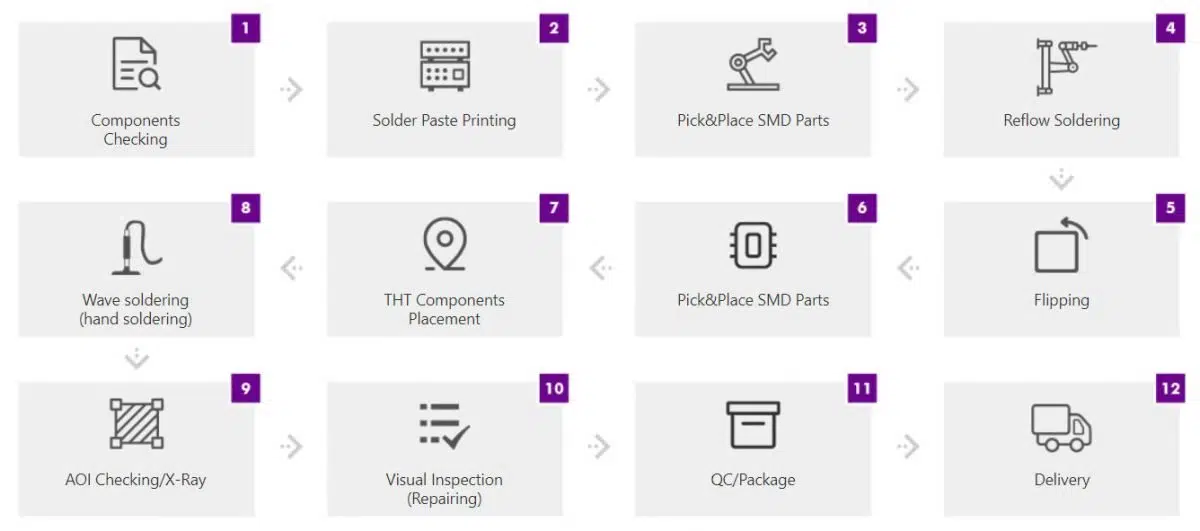
PCB Assembly Process Flow
The PCB assembly process may be a simple one, consisting of several automated and manual steps. With each step of the method, a board manufacturer has both manual and automatic options on which to decide. To assist you in better understanding the PCBA process from start to complete, we’ve explained each step intimately below.
Before the PCB Assembly Process
A few preparatory steps should happen before the real PCBA process even begins. This helps printed circuit board manufacturers evaluate the functionality of a PCB structure, and primarily includes a DFM check. Most companies specializing in PCB assembly need the look file of the PCB to begin out, together with the other design notes and specific requirements. This can be therefore the PCB assembly company can check the PCB file for any issues that will affect the PCB’s functionality or manufacturability. This is often a design for manufacturability check, or DFM check, for short.
The DFM check looks at the least the planning specifications of a PCB. Specifically, this inspection examines any misplaced, redundant, or potentially problematic components. Any of those issues may severely and negatively influence the functionality of the ultimate project. for instance, one common PCB design flaw is leaving insufficient spacing between PCB components. This could end in shorts and other malfunctions.
By identifying possible issues before manufacturing starts, DFM reviews can cut manufacturing expenses and stop unexpected expenses. This can be because these checks block the quantity of scrapped boards. As a part of our commitment to quality at a coffee cost, DFM checks come standard with every JHYPCB project order. JHYPCB provides FREE DFM and DFA ask, however, priceless values because Valor DFM/DFA check JHYPCB depends on an automatic system contributing to high speed and accuracies.
Key Preparation Steps Before PCB Assembly
Before PCB assembly can begin, there are several important steps that must be taken to ensure the successful completion of the project. From component verification to pick and place programming, each of these preparatory tasks plays a critical role in the assembly process. By taking the time to carefully complete these steps, manufacturers can ensure that their PCB assemblies are accurate, efficient, and meet the highest standards of quality. In this article, we will explore the key preparation steps that are necessary before PCB assembly can begin. Here are some of the essential preparation steps:
Parts Procurement: The first step in PCB assembly is to procure all the necessary components required for the assembly process. This involves ordering the correct parts, ensuring they are of the right quality, and verifying that they will work as intended.
PCB Fabrication: Once the parts are procured, the bare PCB must be fabricated according to the design specifications. This involves creating the board, drilling holes for vias and through-holes, and adding copper traces and pads.
SMT Stencil Fabrication: A stencil is required to apply the solder paste to the board. The stencil is typically made of stainless steel and is laser-cut to match the exact location of the pads on the PCB. The stencil is then cleaned and inspected for accuracy.
DFM Check: Before assembling the PCB, a design for manufacturability (DFM) check is performed to ensure that the design is optimized for efficient and cost-effective production. This involves reviewing the PCB design and identifying any potential issues that could impact the assembly process.
DFA Check: A design for assembly (DFA) check is also performed to ensure that the PCB is designed for efficient and accurate assembly. This involves reviewing the PCB design and identifying any potential issues that could impact the assembly process, such as difficult-to-reach components or complex placement sequences.
Component Verification: Before starting the assembly process, it’s essential to verify that all the parts received match the BOM (Bill of Materials) and meet the specifications required for the project. This includes checking for correct part numbers, quantities, package types, and any additional requirements, such as RoHS compliance.
PCB Cleaning: Before assembling the PCB, it should be cleaned thoroughly to remove any dust, debris, or other contaminants that could impact the assembly process or the performance of the finished product.
Solder Paste Inspection: Once the SMT stencil is prepared, it’s important to inspect it carefully to ensure that it’s free of any defects that could lead to solder paste issues during assembly.
Pick and Place Programming: The pick and place machine needs to be programmed to accurately place each component in the correct position on the PCB. This involves creating a pick and place file that contains the component location and orientation information.
By completing these preparation steps, the PCB assembly process can proceed smoothly and with a high degree of accuracy, resulting in a functional and reliable finished product.
Actual PCB Assembly Process Steps
Step 1: Applying Solder Paste Using Stencil
First of all, we apply the solder paste to the areas of the PCB board where the components will fit. This can be done by applying solder paste to the stainless-steel stencil. The stencil and also the PCB is held together by a mechanical fixture and so the solder paste is applied by the applicator evenly to any or all openings within the board. The applicator spreads the solder paste equally. So, a correct amount of solder paste must be employed in the applicator. When the applicator is removed the paste will remain within the desired areas of PCB. The grey color solder paste is 96.5% product of tin and contains 3% of silver and 0.5% of copper and it’s lead-free. This solder paste will melt and creates a powerful joint upon application of warmth in step 3.
Learn more about solder paste Inspection.
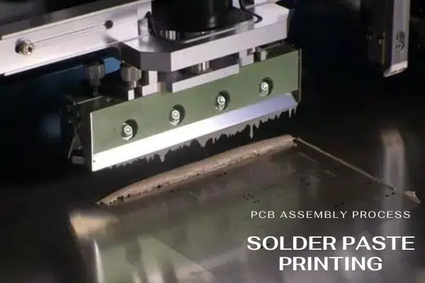
Solder Paste Printing Using Stencil
Step 2: Automated Placement of Components
The second step in PCB Assembly is the automated placement of SMT components on the PCB board. This can be done by using a pick and place robot. At the planning level, the designer creates a file that may be fed to the automated robot. This file has the preprogrammed X, and Y coordinates of every and each component utilized in PCB, and it identifies the placement of all components. Using this information, the automatic robot will only put the SMD devices on board accurately. The pick and place robots will pick the components from their vacuum grip and place them exactly on top of solder paste.
Before the arrival of robotic pick and place machines, the technician will pick the components using tweezers and place them on PCB by carefully viewing the placement and avoiding any jittering hands. This resulted in a high level of fatigue and eyesight weakness in technicians and resulted in a slowed process of PCB assembly of SMT components. Hence the possibilities of mistakes were high. As the technology matured, automated robots for picking and placing components eased the technician’s work and resulted in fast and accurate components placement. These automatic robots can work 24/7 without tiredness.
Pick and Place Machine
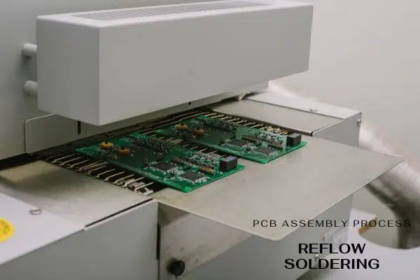
Step 3: Reflow Soldering
The third phase after the parts are placed and solder paste applied is reflow soldering. The reflow soldering is the process where the PCBs together with the components are placed on the conveyor. This belt then moves the PCBs and components in a big oven, which creates a temperature of 250-degree Celsius. These 250 Celsius temperatures are sufficient for the solder to melt. The melted solder will then fix the components upon the PCB and make joints. After the PCB is treated at a hot temperature, it then goes into coolers. These coolers then solidify the solder joints in a controlled fashion. this can create a permanent joint between the SMT component and PCB. Within the case of two-sided PCBs, the PCB side which has fewer or smaller components are going to be treated first from step 1 to three as mentioned above and so comes the opposite side.
Step 4: QC and Inspection
After the reflow soldering, there’s an opportunity that because of some erroneous movement in the PCB holding tray, the components got misaligned and should lead to tangency or open connection. These flaws must be identified and this identification process is termed inspection. Inspection is manual and automatic.
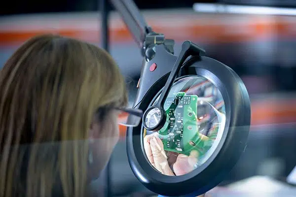
As the PCB has very small SMT components, so visually checking the board for any misalignment or faults may end up in fatigue and eye strains for technicians. So, this method isn’t feasible for advanced SMT boards because of inaccurate results. However, this method is possible for boards having THT components and lesser component density.
For the massive batches of PCB, this method is possible. This method uses an automated machine that has high-powered and high-resolution cameras installed at various angles to look at the solder joints from various directions. The sunshine will reflect the solder joints in numerous angles in step with the standard of solder joints. This automated Optical Inspection (AOI) machine is at an incredibly high speed and takes a very short time to process large batches of PCBs.
The X-ray machine allows the technician to appear through the PCB to work out the inner layer defects. This can be not a typical inspection method and is just employed in complex and advanced PCBs. These review techniques if not correctly used may cause rework or scrap PCB. The inspection needs to be done regular basis to avoid delays, and labor, and material costs.
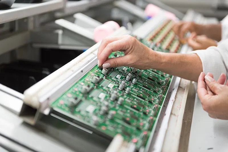
Step 5: THT Component Fixation and Soldering
The through-hole parts are generally found on many printed circuit boards. These components also are referred to as Plated through holes (PTH). These components have leads that will go through the opening within the PCB. These holes connect with other holes and vias by means of copper traces. When these THT components are inserted and soldered in these holes, then they’re electrically connected to another hole within the same PCB because the circuit is designed. These PCBs may contain some THT components and plenty of SMD components therefore the soldering method as discussed above just in case of SMT components like reflow soldering won’t work on THT components. that the two main sorts of THT components soldering or prototype PCB assembly are
The manual soldering method is that common and typically takes longer than compared to the automated setup for SMT. Usually, one technician is designated to insert one component at a time and therefore the board is passed on to another technician who inserts another component on the identical board. Therefore, the board will move all around the line to induce the PTH components stuffed upon it. This makes the method lengthy and then many PCB designs and manufacturing companies avoid using PTH components in their circuit design. But still, the PTH components are the foremost favorite and customary components for many circuit designers.
- Wave Soldering
During this method, once the PTH components are placed on the PCB, the PCB is placed on the conveyor and is moved to a specialized oven. Here a wave of molten solder is splashed on the PCB bottom layer where the components lead is present. This can solder all the pins without delay. However, this method is just for single-sided PCBs and not for double-sided because this molten solder while soldering one side of the PCB can damage components on the other side. After this, the PCB is moved for the final inspection.
Step 6: Final Inspection and Functional Test
Now the PCB is prepared for testing and inspection. This can be the functionality test, where electrical signals and power supply are given to the PCB at the desired pins, and output is checked at the desired test points or output connectors. This test requires common lab instruments like oscilloscope, DMM, and function generator This test is to test the functionality and electrical characteristics of PCB and to verify current, voltage, analog, and digital signals as described within the requirements of PCB AND circuit design If any of the parameters of the PCB shows unacceptable results, then the PCB is discarded or scrapped as per the corporate standard procedures. The testing phase is extremely important because it determines the success or failure of the complete process of PCBA.
Step 7: Final Cleaning, Finishing and Shipment
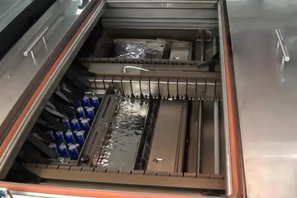
Now that the PCB is tested and declared OK from all aspects, it’s time now to wash the unwanted residual flux, finger dirt, and oil stains. A stainless-steel-based high washing tool using deionized water is sufficient to scrub all sorts of dirt. The deionized water won’t damage the PCB circuit. After washing the PCB is dried with compressed gas. Now the ultimate PCB is prepared for finish off and shipment. After all, products are produced, they’re packaged and shipped in step with customer needs. PCBA electronic product processing may be a relatively complicated process. Within the process of production, each employee must work together and strictly follow the assembly process to manage the standard, meet the customer’s quality requirements, and deliver the right product.

After The PCB Assembly Process
Suffice it to mention, that the PCB assembly process is a grimy one. Soldering paste leaves behind some amount of flux, while human handling can transfer oils and dirt from fingers and clothing to the PCB surface. Once all is finished, the results can look a bit dingy, which is both an aesthetic and a practical issue. After months of staying on a printed circuit board, flux deposition starts to smell and feel damp. It also becomes somewhat acidic, which might damage solder joints over time. Additionally, customer satisfaction tends to suffer when shipments of recent PCBs are covered in residue and fingerprints. For these reasons, washing the merchandise after finishing all the soldering steps is vital.
A stainless-steel, high-pressure washing apparatus using deionized water is that the best tool for removing residue from PCBs. Washing printed circuit boards in deionized water pose no hazard to the machine. This can be because it is the ions in regular water that do damage to a circuit, not the water itself. Deionized water, therefore, is innocuous to the printed circuit boards as they experience wash cycle. After washing, a fast-drying cycle with compressed gas leaves the finished PCBs ready for packaging and shipment.
PCB Assembly Process Flow Chart
What is the difference between SMT, THT and Mixed Technology?
When it comes to PCB assembly, there are different methods to mount components on a board, each with its own advantages and challenges. The most common methods are Surface Mount Technology and Through-Hole Technology, which differ in the way they connect components to the board. Additionally, there is also a third approach called Mixed Technology, which combines SMT and THT for boards with specific requirements.
SMT PCB Assembly Process
SMT is one of the most commonly used PCB assembly processes in modern electronics manufacturing. The SMT PCB assembly process involves placing tiny electronic components onto the surface of a PCB instead of inserting them into holes in the board. This method allows for a higher level of integration and miniaturization, making it possible to produce smaller, lighter and more efficient electronic devices.
The SMT assembly process can be divided into several stages, including:
Stencil Printing: The first step in the SMT assembly process is stencil printing, which involves applying solder paste to the board through a stencil. The solder paste forms the adhesive that holds the components in place.
Component Placement: After the solder paste has been applied, the components are placed on the board using a pick and place machine. The machine is programmed to place each component precisely in its designated location, as specified by the PCB design.
Reflow Soldering: Once the components have been placed, the board is heated in a reflow oven. The solder paste melts and flows to create a permanent bond between the components and the board. This process is critical for ensuring that the connections between the components and the board are reliable and secure.
Inspection: After reflow soldering, the board is inspected to ensure that all components are in place and that there are no defects in the solder joints. Any necessary repairs or adjustments are made at this stage.
Testing: Finally, the completed board undergoes a series of tests to ensure that it is functioning properly. This includes functional testing to verify that the board is performing as expected and any required environmental testing to ensure that it can withstand the intended operating conditions.
Overall, SMT PCB assembly offers a number of advantages over other assembly processes, including greater miniaturization, higher component density, and improved reliability. At JHYPCB, we have extensive experience with SMT PCB assembly and are committed to delivering high-quality, reliable PCB assemblies that meet the unique needs of our customers.
THT PCB Assembly Process
Through-hole technology PCB assembly is an older method of PCB assembly, but it is still used in some applications. Unlike SMT assembly, THT assembly involves inserting leads from electronic components through holes in the PCB and then soldering them to the opposite side of the board. The components used in THT assembly have leads that are designed to be inserted into the holes in the PCB.
The THT assembly process usually involves several steps, including component preparation, component insertion, soldering, and inspection. In the component preparation step, the leads of the electronic components are typically cut and bent to the correct length and shape. Then, the components are inserted into the holes on the PCB. Once the components are in place, the leads are soldered to the opposite side of the board using wave soldering or hand soldering techniques.
After soldering, the board undergoes visual inspection to ensure that all the components are correctly placed and soldered. In addition, automated optical inspection (AOI) and X-ray inspection may also be used to detect defects that are not visible to the naked eye.
THT assembly is typically used for components that are larger or have higher power requirements than SMT components. It is also used for components that require a more secure mechanical attachment to the board. However, THT assembly is generally slower and more labor-intensive than SMT assembly, and it can be more difficult to automate.
Mixed Technology PCB Assembly Process
Mixed technology PCB assembly involves a combination of SMT and THT assembly processes on the same printed circuit board. The process begins with the SMT assembly process, where surface-mount components are placed on the PCB. Next, the THT assembly process begins, where through-hole components are inserted into the PCB and soldered to the traces on the opposite side of the board.
In mixed technology assembly, careful consideration must be given to the placement of through-hole components, to avoid interference with the surface-mount components. After the through-hole components are inserted, the board is inspected for proper placement and orientation.
Finally, the board is sent for reflow soldering, where both the surface-mount and through-hole components are soldered to the PCB. The final step is inspection and testing to ensure that the board is fully functional. Mixed technology assembly requires a high degree of expertise and precision, as well as specialized equipment, to ensure that the final product meets the required specifications.
One-stop Turnkey PCB Assembly manufacturer In China
If you’re looking for a reliable and high-quality PCB assembly service, look no further than JHYPCB. Our comprehensive range of services, including SMT, THT, and mixed technology assembly, allows us to meet the diverse needs of our clients. With a team of experienced engineers and technicians, we are committed to delivering high-quality products, on-time delivery, and exceptional customer service.
Contact us today to discuss your PCB assembly needs and how we can help bring your designs to life. With our expertise and commitment to quality, you can trust JHYPCB to deliver the best PCB assembly services for your business. Let us be your one-stop-shop for all your PCB assembly needs.
Related Reading
- What are the Advantages of a Prototype PCB Assembly?
- Why Choose China PCB Assembly Manufacturer?
- What are the Benefits of Turnkey PCB Assembly?
- How to Choose a PCB Assembly Manufacturer?
- Small Batch PCB Assembly Essential for Prototyping
- SMD Vs. SMT, what is The Difference?
- How to Reduce Your PCB Assembly Cost?
- What Is PCB Assembly Drawing?