


PCB Manufacturing Services
Heavy Copper PCB, Thick Copper PCB Fabrication Service
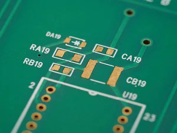
Heavy Copper PCB Overview
With the event of society, there’s an excellent demand for heavy copper PCB. Now heavy copper PCBs are widely utilized in various electronic industries. In general, heavy copper technology can realize complicated switches in limited space combining the circuitry for prime current levels, also as is nice for warmth dissipation. Multilayer and double-sided are the foremost common designs we all know. What’s more, heavy copper PCB technology makes it possible to mix great layout structures on the external layers and heavy copper layers within the internal layers.
What is Thick Copper PCB?
What is Heavy Copper PCB?
Heavy Copper PCB Board Thickness
Heavy copper PCB is a printed circuit board with a copper thickness that's ≥ 3oz per sq. ft in its outer and inner layers. What makes a circuit board classified as a heavy copper PCB is its thicker plating. During the assembly of heavy copper PCB, copper thickness is enhanced through plated holes and sidewalls. For instance, when a printed circuit board has 2 oz of copper per sq. ft width, it's a regular PCB. However, if it's over 3oz of copper, it's a heavy copper PCB. Heavy copper PCB is taken into account as a reliable wiring option. Heavy copper PCB is different from exciting copper PCB which structures within 20 oz to 200 oz per sq. ft.
Heavy Copper PCB Applications
Heavy Copper PCBs are manufactured with 4 or more oz of copper on each layer. 4 oz Copper PCBs are most ordinarily utilized in commercial products. The copper concentration is often as high as 200 ounces per square measure. Heavy Copper PCBs are widely utilized in electronics and electrical circuitry where high power transmission is required. Additionally, the warm strength presented by these PCBs is perfect. In many applications, especially electronics, the thermal range is of significant importance since the warm temperature is devastating for sensitive electronic components and badly affects circuit performance.
Heat-sinking Capacity of Heavy Copper PCBs
The heat-sinking capacity of Heavy Copper PCBs is far higher compared to casual PCBs. Heat sinking is vitally essential for the event of a strong and sturdy circuit. Poor handling of warmth signals not only affects electronics performance but also shortens the lifetime of circuitry.
How is Heavy Copper PCB Fabricated?
For the fabrication of heavy copper PCB, plating or etching is commonly used. The most aim is to feature copper thickness to sidewalls and plated holes. The methods employed in fabricating heavy copper PCB aren’t far-fetched. Heavy copper PCBs need special etching and plating methods to confirm the additional thickness of copper. Using the conventional etching techniques for the fabrication of heavy copper PCBs isn’t ideal. Normal design methods produce over-etched margins and edge outlines that are rough. PCB producers now use advanced etching and plating methods to attain straight edges.
During the PCB manufacturing procedure, heavy copper printed circuit boards are electroplated. This can help thicken the walls of PTH on the PCB. With this system, the layer count shrinks, and therefore the impedance distribution reduces. When PCBs are exposed to many cycles during the manufacturing process, the plated holes can become weak. The fabrication of heavy copper PCBs has its limitations which include:
- The etching process increases the value
- The etching process requires an enormous amount of copper to be removed
- It is hard to fabricate finer lines and thick copper traces
- Heavy copper drops make the outward rough
Methods for Fabricating Heavy PCBs
JHYPCB utilizes different techniques for fabricating heavy copper PCBs.
- Embedded copper method
This method fabricates heavy copper PCB employing a flat surface. Here the heavy copper is inserted within the prepreg resin. The width of the resin limits the width of the copper. For instance, the fabricator begins with a 6-mil laminate and a 1 oz copper clad. Then the copper clad is roofed with a photoresist. After this, a 5-mil light beam is employed to chop the circuit pattern from the side of the laminate. The laser needs to cut via the laminate to the copper foil. If the laser is controlled, the fabricator can prevent the copper foil from being damaged.
The fabricator positions the laminate into a plating tank to electroplate. The copper plating produces about 6 mil plating thickness after filling the laser-cut groove on the laminate.
- Blue Bar Method
The blue bar technique contains inserting heavy copper bars into circuit boards. This method saves the fabric and reduces the burden of the PCB. During the fabrication process, the resin flows into space within the copper traces, this helps to realize an excellent top surface.
Fabricators must listen to the amount of copper filling between inner layers when it involves multilayer boards with heavy copper layers. Low levels of fill and low levels of resin can result in resin hunger.
What does Heavy Copper PCB offer?
Heavy copper PCB incorporates a lot to supply. It’s got some unique features that make it a perfect option for high-end applications. Let’s discuss a number of the advantages of this PCB;
Great Thermal Distribution:
Thanks to its copper-plated vias, this PCB offers high thermal resistance. Heavy copper PCBs are employed in applications that demand high speed and high frequency. You’ll also use this PCB at harsh temperatures.
Mechanical Strength:
Heavy copper PCB features great mechanical strength. When this PCB is employed, it makes the electrical system durable and robust.
Good Conductor:
Heavy copper circuit boards are an honest conductor. They’re utilized within the production of electronics because of this feature. They assist to link various boards together. These boards can transfer current.
Onboard Conductor:
Heavy copper boards offer an onboard heat sink. With these boards, you’ll achieve effective heat sinks on mosaic surfaces.
Great Dissipation Factor:
Heavy copper PCBs are ideal for big components with a high loss of power. These PCBs avoid warmness from occurring in electric systems. They dissipate excess heat effectively.
Supports Exotic Material:
Heavy copper helps to guard and enhance exotic material. Unusual materials are occasionally used for designing electric components. A warm temperature may have an exotic material. Heavy copper boards end circuit letdowns because they use an unusual substantial to its full abilities.
Benefits of Heavy Copper PCB
Heavy copper PCB comes with many benefits. Thanks to its unique features, it's become an ideal option for high-end applications. Here are the benefits of heavy copper PCB.
Due to their copper-plated vias, heavy copper PCBs provide good thermal distribution. Hence, they're employed in applications that need high frequency and high speed. The PCB is utilized in harsh temperatures.
Another advantage of heavy copper PCB is its excellent mechanical strength. This makes it more durable and robust.
Heavy copper PCBs are perfect for significant elements with a high loss of power. This is often because they need a superb dissipation factor. They prevent overheating from happening in electrical systems.
A heavy copper PCB is a wonderful conductor. Hence, the PCB is employed to supply various electronics because of this benefit. it's possible to link several boards together so that they can quickly transfer current.
Features Of Heavy Copper PCB
Here are some features of Heavy Copper PCB:
- Copper Weight
This is often the most distinguishing feature of heavy copper PCBs. Copper weight refers to the load of the copper utilized in an area unit area. This weight is sometimes measured in ounces. It indicates the copper’s thickness on the layer.
- Outer Layers
These confer with the external copper layers of the board. Electronic components are usually bonded to the external layers. The external layers begin with copper foil which is coated with copper. This helps to extend the thickness. The copper weight of the external layers is preset for normal designs. Heavy copper PCB manufacturers can alter the load and thickness of the copper to fit your requirement.
- Inner Layers
The dielectric thickness, moreover because of the copper mass of the inner layers, is predefined for quality projects. However, the copper weight and thickness in these layers are often adjusted to support your needs.
Heavy Copper PCB Capabilities
It is important to contemplate the capabilities of heavy copper PCBs when using them for a few applications. This kind of PCB is costlier to provide support to their requirements. A Heavy copper PCB should have these capabilities:
- A minimum board size of 6mm by 6mm and a maximum board size of 457mm by 610mm
- Copper thickness is larger than 3oz for every sq ft.
- A board thickness between 0.6mm and 6mm
- Maximum external layer copper weight should be 15oz
- Solder mask color should be either green, blue, red, black, white, purple, or yellow
- Silkscreen color is white, yellow, or black
- The surface finishing should be Immersion Gold, OSP, and HASL
- The finished thickness is between 0.020 inches and 0.275 inches
Applications of Heavy Copper PCB
Heavy copper PCB offers some outstanding features that make it ideal for sure applications. This kind of PCB is employed in military and defense applications. The demand for heavy copper PCBs has been increasing over the years. This is often because these PCBs are utilized in several applications such as:
- Rail traction systems
- UPS systems
- Solar power converters
- Nuclear power industries
- Automotive industries
- Torque controls
- Power line motors
- Welding equipment
- Military equipment
- Safety and signal systems
- Protection relays
Difference Between Standard PCB and Heavy Copper PCB
- Standard PCBs are quickly produced with copper etching and plating processes. The boards are plated to extend copper thickness to traces and planes. Also, the quantity of copper employed in standard PCBs is 1oz. On the opposite hand, there are different manufacturing methods for heavy copper PCBs and therefore the amount of copper used is quite 3oz.
- With the quality printed circuit boards, CNC cutting, copper etching, and plating methods are utilized. But heavy copper PCBs are obtained through various etching and step plating methods.
- Standard PCBs perform lighter duties while heavy copper printed circuit boards perform heavy tasks. Also, the quality ones conduct a lower current while the heavy PCBs conduct a significant current.
Conclusion
Heavy copper PCBs are produced via etching and plating methods. The foremost aim of the production of this PCB is to feature copper thickness through sidewalls and plated-through holes. Heavy copper PCBs have several benefits which make them in high demand.
Due to their outstanding features and benefits, they’ll meet your electrical requirements. These circuit boards will always dissipate heat generated thanks to heavy currents conduction. Electronics using heavy copper boards are in use for a protracted time. Heavy copper can carry high currents. These boards will still meet the wants of assorted applications.
High power circuit wirings are often developed using Heavy Copper PCBs. Such a wiring mechanism offers more reliable thermal stress handling and offers fine finishing while incorporating multiple channels on one layer of a compact board.
Heavy Copper PCBs are widely employed in various products as they supply multiple features for improving circuit performance. These PCBs are widely utilized in high-power equipment like transformers, heat sinking, power inverters, military equipment, solar panels, automotive products, welding plants, and power distribution systems.
Heavy Copper PCB generally has to adopt a special pressing procedure. It involves the employment of multiple PP fillings to satisfy the specified filling during the pressing process. The pressing involves a high and an outsized flow of glue. There are empty areas within the heavy copper PCB in each layer of the inner layer pattern; there’s no copper within the open area. Also, the sting of the plate is intended with one air guide groove.
Due to the high, the quantity of PP glue passes very easily, and also the air guide grooves are lost. This causes the thickness of the board within the open area to be too thin. The board’s overall thickness is extremely large, which causes the film to be not tight during the following processing of the outer layer, ultimately causing the merchandise to be not useable.
The priority is to scale back the glue flow within the open area and forestall the open area’s thickness from being too thin. This is often an urgent problem to be solved within the production process for such heavy copper PCB.
Related PCB Fabrication Services

Related Reading
Are you looking for a heavy copper PCB or a thick copper PCB manufacturer? You can use the heavy copper PCB online quote request form to inquire about heavy copper PCB fabrication for your applications. As a professional heavy copper PCB manufacturer in China, we can provide 4 oz copper PCB, 8 oz copper PCB, 10 oz copper PCB, or Extreme Copper PCB fabrication service. You can email us Gerber files and information on PCB volume and others at sales@pcbjhy.com or call us at (0086) 13825274100.