


ORDER GUIDE
What Files are Needed for PCB Assembly
PCB Assembly Files List
After the manufacturer manufactures the PCB, it needs to be brought to a PCB assembly factory for assembly. JHYPCB is a reliable PCB assembly manufacturer; we need you to provide Gerber/ODB++, Pick-and-place file, BOM, Assembly Drawing, etc., to start your PCBA work.
Please send us the files in the correct format and compress them as .zip/.rar. You will have two ways to send these files to us, either through our web form submission or by sending an email to sales@pcbjhy.com.
Upon receipt of your documents, we will review them to ensure that all information on the assembly is complete and accurate.
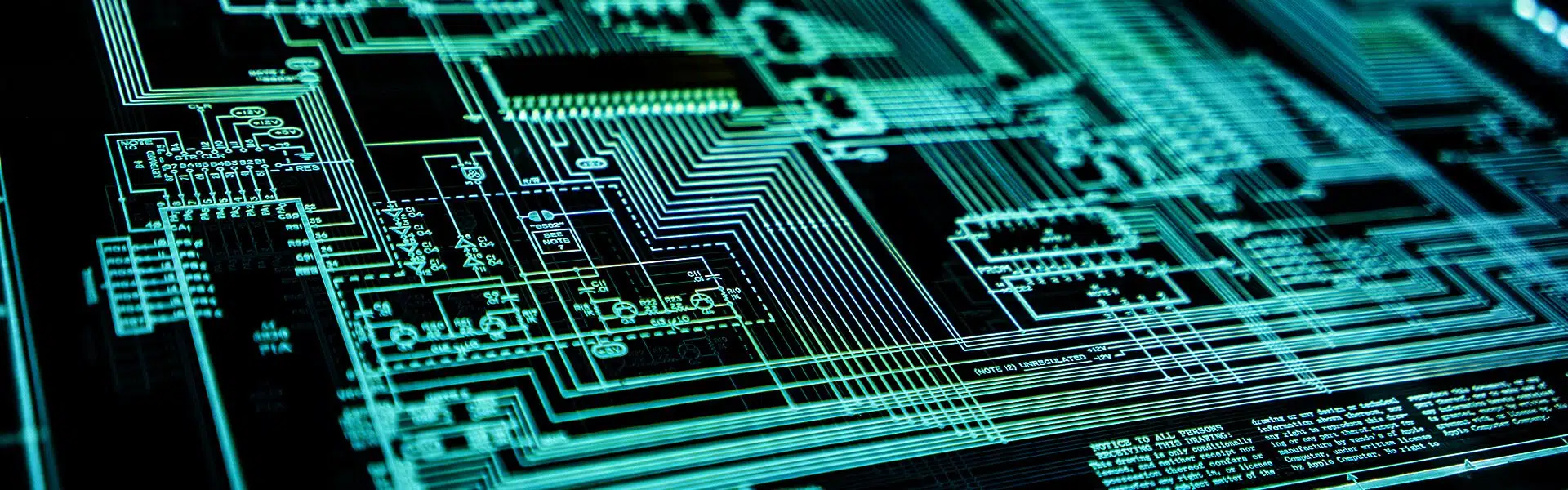


Gerber File
Gerber files are helpful in both printed circuit board manufacturing and assembly processes. Gerber file contains all layers of the PCB stack, such as the Top layer, Bottom layer, Solder mask top/bottom layer, silkscreen top/bottom layer, etc.
RS-274D and RS-274X are the most common file format types for Gerber. RS-274D is called Standard Gerber, and RS-274X is called Extended Gerber.
The Gerber files that JHYPCB accepts are RS-274X, .PCBDOC, PCB, Eagle file, etc.
Available EDA tools, including KiCAD, Allegro, and Altium Designer, can help generate and export Gerber files.
The role of Gerber files in PCB assembly is for the production of SMT stencils.
Click here to learn more about PCB fabrication files.

Bill of Materials (BOM)
Bill of Materials lists all the components that will be included in the assembled PCB. The BOM is basically a large table, where each row in the table corresponds to a specific component that will be procured from a distributor or component manufacturer. Each entry in a BOM needs to include some specific information:
- A short description of the component
- Which reference designators are assigned to the component
- The quantity of the component used in the assembly
- The component manufacturer and the MPN
- The distributor/supplier where the component can be purchased
- The distributor/supplier’s internal part number (this is often a slight variation on the MPN)
- The component’s footprint or packaging
Some designers may prepare a BOM that includes alternative distributor information so that the part can be procured if the primary distributor does not have inventory.
It is also a standard practice to include components in a BOM that will never be placed on the PCB. When this is done, the line in the BOM is marked “DNP” (meaning “do not populate” or “do not place”) or “DNI” (do not include). This designation tells the assembler to ignore that particular line in the BOM.
There are several reasons for doing this. Sometimes, these are mechanical components like brackets, standoffs, or fasteners. The most common reason is when a design has multiple variants that have optional components. Another example is seen in some families of ICs that use configuration resistors or capacitors. Some ICs within the same product line will use these components to configure the device into specific modes, and it is common to just create the PCB layout so that it can accommodate any device mode. The designer can then mark the un-needed components DNP/DNI in the BOM.
BOMs can also be generated and exported in EDA tools like KiCAD, Allegro, and Altium Designer.
Learn more: What is the BoM of a PCB Assembly?
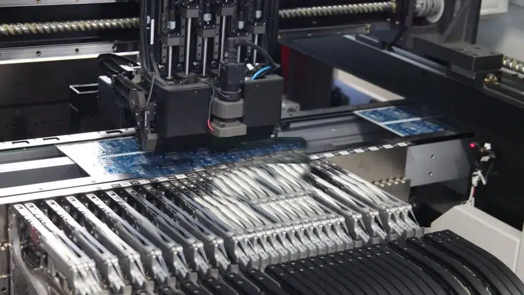
Pick-and-Place File
The Pick-and-Place file, also known as centroid file or XY Coordinate file.
A pick-and-place file contains component placement instructions that are used in the assembly process. This file will contain coordinates for each component in the PCBA so that it can be placed with automated assembly equipment, called a pick-and-place machine. This equipment will use a pick-and-place file to locate and place components on the board before the board passes through soldering. Once placed, the board will pass through wave/reflow soldering, and the assembly process will be completed.
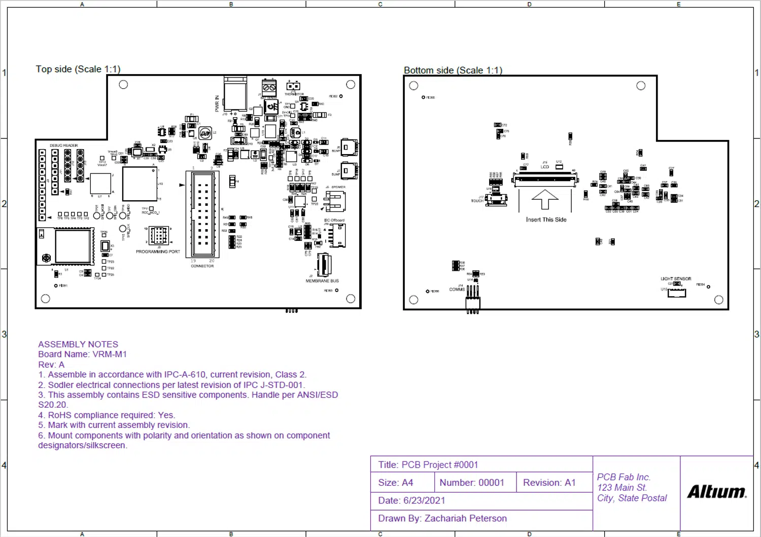
Assembly Drawing
Just to make sure there are no mistakes or delays in PCB assembly, it is a good idea to prepare Assembly drawings to show just the basic component location and orientation information.
An assembly drawing is not always required, but it is useful in a similar way as a fabrication drawing. An assembly drawing includes a scale drawing that shows the locations of components and their designators on the top and bottom sides of the board. The idea is to summarize the location and orientation of components. Additional requirements are included in a set of assembly notes.
An assembly drawing includes the following:
- Pictorial representation: An outline of the board showing the component locations and corresponding reference designators.
- Assembly details: Included when there is a space restriction in the pictorial to explain densely packed regions or small parts.
- Assembly notes: Help the assemblers with information like the designation of primary side, mounting instructions, soldering instructions, specialized assembly methods, height restrictions of the board, cable orientation, etc.
Assembly drawings are often automatically generated from PCB design CAD tools like PCB fabrication drawings.
At JHYPCB, we prefer assembly drawings in .pdf format.

3D files
Some of the ECAD tools can generate step files from the design files. Step files give a 3d view of the design. We can visually check the placement of the components. This is especially useful to check whether the direction of the connectors is correct.
Final
To assemble your printed circuit board correctly and quickly, we strongly recommend you provide us with all documents or information related to the circuit board, including assembly drawings, special assembly instructions, 3D files, etc. This information is beneficial for us to understand your assembly needs better.