


PCB Fabrication Services
Double-Sided PCBs
What is Double Sided PCB?
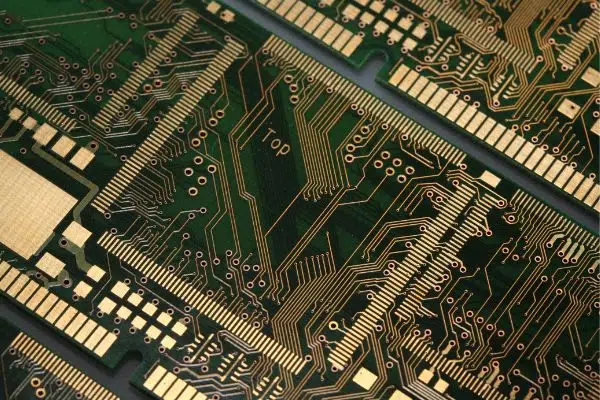
Double Sided PCB or Double Layer Printed Circuit boards are the gateway to higher technology applications. They permit for closer (and perhaps more) routing traces by alternating between a top and bottom layer using vias. Today, double sided printed circuit board technology is the foremost popular kind of printed circuit board within the industry. Double-Sided PCB or Double Layer printed circuit board is no more complex than Single-Sided PCBs. These kinds of PCBs have one single layer of the bottom substrate but a conductive (copper) layer on each side of the substrate. A solder mask is applied on either side of the board.
Holes for electronic components should be plated through for conductivity on both circuits. Conductive holes within the PCB allow circuits on one side to connect to circuits on the opposite side. Electronic components are soldered on either side. Since there are two or double conductive layers forming the circuit; it’s called Double Sided PCB or Two Layer PCB. Both through-hole electronic components and Surface Mount Components (SMD) are soldered on either side of this kind of PCB. SMD components are soldered with Surface Mount Technology.
To use circuits on each side, there must be a correct circuit connection between the 2 sides. The “bridges” between such circuits are called vias. A via is a small hole on the PCB board filled or coated with metal, which might be connected with the circuits on either side. Because the realm of the double-sided board is twice as large as that of the single-sided board, the double-sided board solves the issue of the single-sided board because of the interlaced layout (it is connected to the opposite side through the holes), and it’s more suitable for more complicated circuits than the single-sided board.

People need electronic products with high performance, small size, and multiple functions, which promotes the event of printed circuit board manufacturing to be light, thin, short, and small. With limited space, more functions are realized, layout density has become greater, and therefore the hole diameter is smaller. The minimum hole diameter of mechanical drilling capacity has dropped from 0.4mm to 0.2mm or perhaps smaller. The outlet diameter of the PTH is getting smaller and smaller. The standard of the PTH (Plated Through Hole) on which the layer-to-layer interconnection depends is directly associated with the reliability of the printed circuit board.
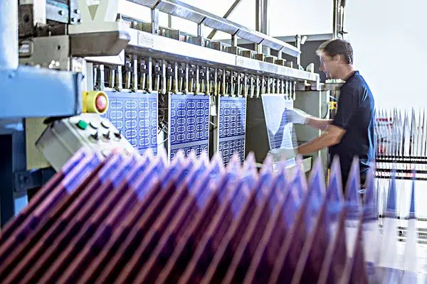
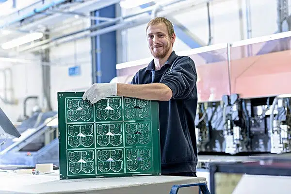
Double Sided PCB Manufacturing Proces
Planning and Preproduction
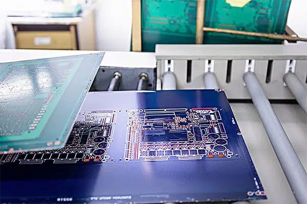
JHYPCB is a leading PCB manufacturing service provider in China, we have been committed to providing customers with high reliability PCB manufacturing services.
Before manufacturing, the JHYPCB checks the Gerber Files and other details like films, mechanical drawings, and specifications.
- Number of boards per mother panel
- Decide the panel size for the foremost economical reason
- Features and knowledge to be added during panelization. Like UL symbols, test coupons, layer numbers, and borders are selected at this point
- Layer materials
- Drilled hole sizes
- Tooling holes or target locations
Double-sided PCB Manufacturing Procedure
The following passage explains the stages involved in creating a double-sided board with a solder mask over bare copper (SMOBC), plated through-holes (PTH), gold-plated connections, and the part legend.
1. Preparing Material
Using the knowledge of the traveler- including the numbers and sizes of the panels, furthermore as any special instructions, the manufacturer prepares the materials necessary to process the order. PCBs start with copper-clad epoxy glass because of the stuff. There are lots of materials utilized in PCB manufacturing for users and printed circuit board manufacturers to decide on from. Different brands and materials have different characteristics, and different materials also provide different benefits, like FR4, a ceramic substrate, iron substrate, aluminum substrate, etc.
Fr-4 is one of the flame retardant materials widely employed in PCB base substrates. FR4 board is economical and affordable and might maintain the soundness and safety of the PCB board under heat conditions. However, FR4 isn’t suitable for high-frequency and high-speed PCBs. Now, JHYPCB wants to settle on high-frequency materials, like Rogers’RO4000 series, RT5000/6000 series, Tacanic’s TLX series, etc. Aluminum, metal, or copper is used in the LED industry because the substrate for LED PCB or aluminum PCB is utilized.
2. Cutting of CCL (Copper Clad Laminate)
The next step is to chop the board in step with the necessity. The raw PCB board is kind of large. There are various sizes available, like 37 x 49 inches, 41 x 49 inches, and 43 x 49 inches. Therefore, it’s cut within the required sizes which will be employed in the machines. The board size obtained after cutting isn’t in keeping with your circuit size; it’s much larger. Your PCB size might be small, so multiple circuits on the board can make the method economical.
3. Drilling
The board goes to an automatic drilling machine that makes holes within the board quickly. The machine changes the drill bits on its own; everything is automated.
4. Deburring
As drilling processes improve, burr-free holes are often produced. But most manufacturers process drilled panels through a deburring machine. The panels taste brushes or abrasive wheels that mechanically remove any copper burns at the rims of the holes. Deburring also removes any fingerprints and oxides to form a smooth, shiny surface.
5. Electroless Copper Deposition (Plating Through Holes, PTH)
Electroless deposition of Cu through the holes as holes are composed of epoxy initially. After Cu deposition, the panel is dipped in acid dip and anti-tarnish solution to forestall oxidation. it’s of two types- horizontal and vertical. Horizontal PTH is for carbon deposition and vertical PTH is for Cu deposition. Electroless copper is one of the foremost important steps in double-sided PCB and multilayer PCB manufacturing processes. Because all PCBs with 2 or more layers use plated through holes to attach the conductors between the layers.
6. Photo Imaging
In photo imaging, a negative image circuitry design is transferred to the PCB panel. First, the panel is roofed with a layer of photoresist. The foremost common photoresist material is dry film plating resist is an ultraviolet (UV) light-sensitive photopolymer. It’s supplied on a roll and applied by processing the panel through heated rollers on a hot roll laminator. Once the film is applied, the board is prepared to be exposed to UV light for circuit printing.
The whole process is distributed in a very room where there are only yellow lights. It’s because photo-resistive films are sensitive to other lights. The film that has the circuit design is applied over the board; it’s applied on either side. Then, the board passes through a UV light chamber. When the board is exposed to UV light, the circuit part is hardened, while the excessive part remains identical.
7. Pattern Plating
First, the panels are clamped in plating racks and immersed during a series of chemical baths that clean the copper pattern that creates up the circuitry. Next, the panels are immersed in a copper plating solution. The solution and panels have opposite electrolytic charges. These opposite polarities cause copper ions to migrate to the uncoated copper areas on the panel, depositing the specified thickness of copper on the plate’s surface and within the holes. After copper plating, the panels are moved from bath to bath. The circuitry pattern is roofed with extra copper and is further electroplated with tin or tin/lead solder.
8. Developing and Etching
The panels are placed in a very tank or spray machine to get rid of the imaging material. This step is additionally called resist stripping. After the resist is stripped off, the panels are placed within the conveyorized spray etcher or batch tank, where a chemical etchant (an ammonia-based compound) removes the uncovered copper but doesn’t attack the tin or tin/lead plating, which protects the copper underneath. The tin or tin/lead plating is named the etch resist. Then the tin or tin/lead is chemically stripped from the copper, revealing the copper circuitry pattern.
9. Solder Masking
Green, white, blue, and other colors of solder mask on the circuit is a thin layer of polymer that works as an insulator between two conducting lines. It prevents the formation of short circuits. The mask is applied everywhere on the board, then it’s dried. Remove the surplus solder mask that’s over the circuit. A movie that contains circuit patterns is applied over the board. Then the board goes through a UV chamber. The solder apart from the circuit is hardened while the solder mask over the circuit remains identical. Finally, the solder mask over the circuit is cleaned.
10. Surface Finishing
The copper on the board can undergo oxidation. It cannot last for an extended time. Therefore, it’s necessary to use a surface finish over copper to guard it against oxidation. There are many varieties of surface finishes available, and customers can pick consistent with their needs. You’ll be able to choose HASL, OSP, ENIG, ENEG, ENEPIG, Immersion tin, Immersion silver, etc.
11. Gold and Nickel Plating
Other plating finishes are used, most ordinarily gold. However, copper and gold tend to undergo solid-state diffusion into one another (with copper doing so at a faster rate); the method is accelerated by increased temperature. Copper on a tracing surface oxidizes, leading to increased contact resistance (copper migrating into the gold can cause the gold to tarnish and corrode). This could be minimized by placing a barrier layer between the copper and gold. Nickel is usually used as a barrier layer to forestall the gold migrating into the copper on the tracks. (The nickel barrier helps to scale back both the amount and also the effect of pores compared with plating gold directly over the copper base.) The nickel protective coating provides several benefits. It is backing to the gold for extra hardness moreover as provides a good diffusion barrier layer between gold and copper. The nickel/gold provides a finish that’s heat and corrosion resistant, environmentally stable, wire solderable, and sturdy (the nickel underplate enhances the wear and tear characteristics of gold) albeit at a better cost than simple solder finishes. Traditionally, nickel/gold plating has been applied over copper tracks used for keyboard contacts or edge fingers to supply the conductive, corrosion resistant coating. This approach provides benefits for soldering.
12. Applying the Component Legend
The labels on the PCB are called silkscreens. These will be accustomed mark components and inserting the brand. During this step, the PCB board enters into an enormous printer that prints the labels on the board. Silkscreens are available in various colors, like red, blue, yellow, and black, but the quality color is white.
13. Separation or Cutting
A cutting machine or instrument is used to cut the circuits and makes them apart pieces.
14. Electrical Testing
For this purpose, the Flying Probe Test is employed. It’s an easy test during which there are multiple probes. The probes are placed over the connections, and also the current is gone through them. It checks whether the circuit is functioning for sure or not. As an example, if there’s no connection between two paths, then the present shouldn’t pass if the probes are connected to them.
Benefits of Double layer PCBS
- Increased circuit density
- Intermediate level of circuit complexity
- Reduced board size (which can reduce costs)
- Provides more flexibility
- Advanced circuit density
- Reduced board size
- Optimum service of available space as there is space for parts on both sides of the board
- Can be used in multiple electronic devices
- More complex projects can be created
- Expense effective
Applications of Double Layer PCBs
There are nearly endless applications for old and new methods. Fine line surface mount, ultra-high copper build, high and low temperature, Solder coated, silver, and gold finishes are just a few examples of double-sided PCB applications.
The followings are the applications in which Double-sided PCBs can be used:
- Industrial controls
- Used in big plants
- Power supplies
- Converters
- Control relays
- Instrumentation
- Regulators
- UPS systems
- Power conversion
- HVAC
- LED lighting
- Hard drives
- Printers
- Phone systems
- Power monitoring
- Automotive dashboards
- Line reactors
- Test equipment
- Amplifiers
- Traffic systems
- Vending machines
Related PCB Fabrication Service
Related Reading
- PCB Fabrication and Assembly Services Manufacturer In China
- What is PCB Panelization and its Methods in PCB Manufacturing?
- Outer Layer Processing of PCB Fabrication Process
- Inner Layer Processing of PCB Fabrication Process
- PCB Design For Assembly (DFA) Inspection & Review Checklist
- Decoding DFM Evaluation and Analysis
- What is the PCB Fabrication Process?