


PCB Assembly Testing and Inspection Services
Flying Probe Testing for PCB Assembly
Overview
We all are aware of printed circuit boards (PCBs) are the core of electronic product functionality. These PCBs consist of the hard green color board commonly seen all told equipment when it’s opened inside. These PCBs are fully loaded with electronic components like resistors, capacitors, ICs, inductors, transformers, chokes, jumpers and connectors, and plenty of other stuff. The components together with PCB copper tracks are connected with one another and designed to hold out one or quite one function.
Flying Probe Testing for PCB Assembly: All You Need to Know
What Is Flying Probe Testing?
To ensure the quality of the finished PCB assembly, various testing and inspection methods are adopted. The flying probe test is one of the PCBA testing and inspection methods.
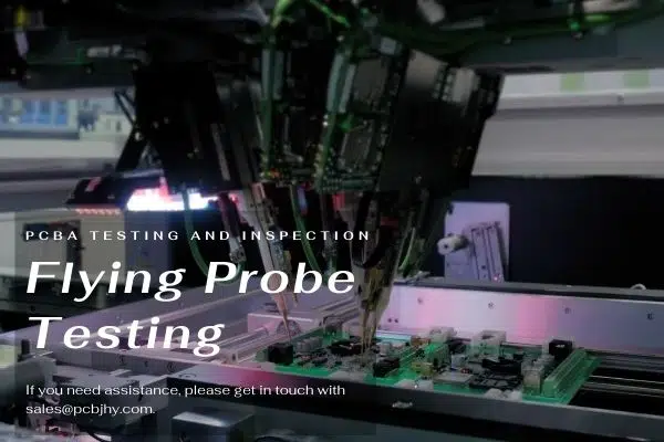
Flying probe testing, because the name implies uses test probes that “fly” i.e., the test probes move from test points to other test points as per instructions given by the precise software program that’s written for the board under test. No custom fixture is required, so it could even be called a fixtureless in-circuit test if used on an assembled PCB. Hence, it’s highly cost-effective for prototypes and low to mid-volume production. The flying probe testers originally evolved to be used just for bare board testing, and they became the de-facto standard for bare-board testing (which involves testing for shorts, opens, etc. between copper conductor features on the bare PCB) where the most electrical parameter that’s measured is that the resistance between two points or nodes.
All the FPT gives a Test Program Generating Software that can be run on a personal computer. This application requires the PCB assembly’s BOM and also the ECAD file. The Gerbers alone don’t seem to be sufficient for this; the ECAD file must be an intelligent CAD file, which suggests that it should be either in ODB++ format or IPC-2581 format, or local ECAD pattern file format as per the ECAD application tool (e.g., Allegro or Altium or PADS, etc.) that was employed in designing the PCB. The BOM has to be in an EXCEL format.
Once the test program is generated, it’s loaded into the FPT tester. The circuit card assembly to be tested, which might be either one board or an array of boards, is placed on a conveyor belt so it can travel inside the tester area where the probes are. When the test program is run, the probes, under the control of the test program, will contact the pads (component pads and test pads if any), and therefore the unmasked vias as per the test program already supplied to the tester, and the tester will apply electrical test signals and give potential to the probe points and assemble all the measurements thereof.
These measurements are going to be processed inside the tester to seek out if the circuit portion within the probes is giving expected results (as per components there) within already specified tolerances. During this manner, FPT detects the defects of that unit. FPT hardware is supplied with signal generators, dc and ac power supplies, various styles of sensors, a multiplexing system, digital multimeters, frequency counters, etc. Which are wont to provide signals to excite the PCB nodes and to form measurements on the nodes of the components and interconnections on the PCB assembly.
By a fancy scheme of excitation signals, FPT tries to isolate, as far as feasible, the component segments between the testing probes from the remainder of the interconnections to other components on the board. This “virtual isolation” of components from the remainder of the circuit interconnections makes it possible to live component values as accurately as feasible, while they still remain connected within the circuitry on the board.
Steps Use in This Method
To implement flying probe test programming, testing staff should first transform CAD (computer-aided design) data provided by engineers into an applicable file. Then, the newly-generated file is run through a test program with new files with corresponding formats generated. Last, all the files are going to be created catering to UUT test demands and requirements.
As soon as test programming is completed, the original flying probe test is around the corner. A testing item should be determined first, shorts as an example. Then, information on mentioned points conforming to UUT should be picked up from CAD data. As shortly as UUT is fixed on the program, the programming is going to be dispensed to inspect the fabrication or assembly matters. It’s necessary to mean that debugging should be done before official testing. What’s more, debugging of flying probe test are often completed within a shorter time compared with conventional ICT test.
- The apparatus utilizes an XY grid, gotten from fundamental CAD (ASCII or ODB machine files). Coordinates are programmed to match the printed circuit.
- Needles come down at a 45-degree angle. The prober needs two access points on the board to make connections.
- The machine programmer figures out the worth and sets it. The machine then verifies that value.
- The test may show you wish to the Venice a circuit. this suggests you’ve got some interconnecting circuits that can’t immediately be worked out, so you pull components out of the circuit and theorize what’s occurring with the remainder of the circuit.
- Flying probe tester carries out programming more easily and more quickly than traditional ICT (in-circuit test) systems, flying probe test for instance.
Flying Probe Testing for PCB Assembly
What Are The Benefits of Flying Probe Test?
- Cheaper and faster to implement or modify. No fixture is required.
- Higher trail coverage is able to utilize vias and part pads as test points.
- No have to add test points. Save board space.
- No need for test fixtures for every PCB variant
- A well organized and quick way of testing mass-produced products
- The short test development cycle
- Relatively low-test cost
- High conversion flexibility
- Rapid feedback was provided to PCB design engineers during the prototyping period.
Disadvantages
- The test jig is a further expense.
- Not suitable for little batch production or prototyping as any changes to the planning requires the test jig to be modified/re-made.
- Can only access test points, the designer has to add test points to the board.
- Cannot estimate certain defects, e.g., excess or insufficient solder, voids.
- A flying probe test cannot look at ball grid arrays (BGAs)