


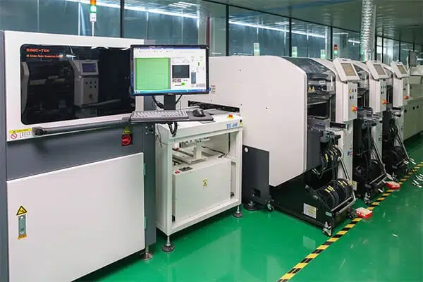
PCB Assembly Inspection
What Is Solder Paste Inspection (SPI) For PCB Assembly, And Why Is It Important?
What Is Solder Paste Inspection?
Solder paste is essentially a mixture of two components, mainly flux and powdered metal. The metal used in the mixture has a low melting point so that it can melt easily. Usually, you will see silver, zinc, copper, bismuth, or tin in the solder paste. If you look into solder paste via microscope, you will see small metal balls. The size of these balls ranges from 20 to 38 microns.
Flux not only acts as a carrier for the metal, but it is also responsible for cleaning surfaces by removing oxides and impurities. It removes the oxide film that is created on the surface of metals. It makes the surface ready for the soldering process.
The work of solder paste is to create a bond between two metals. It creates a bond between the component and the PCB without melting the metals that are being joined together. After soldering, it not only creates a metallic joint of the component with PCB, but it also creates an electrical connection.
PCB Assembly Inspection
What Is Solder Paste Inspection (SPI)?
Solder Paste Inspection (SPI) is a process to check and analyze solder on the PCB board. It is an important process for the whole assembly because it identifies defects in the earlier stage. It can also measure the volume and shape of the deposits of solder paste.
Early identification of any defect means it will be identified at the right time. Although there will be a cost to eliminate the issue, it will be much less than in the later stages.
If Solder Paste Inspection is not done and a defect is identified after reflow, it will take 10 times more time and money to rectify the issue.
There are two techniques for Solder Paste Inspection, Automated Optical Inspection (AOI) and Automated X-Ray Inspection (AXI).
Automated Optical Inspection (AOI)
AOI is an inspection method that detects the defects in the PCBs automatically. The technique is quite fast, which is why it is preferred for bulk PCB Assembly manufacturing.
It can detect different faults, including component defects, dimensional defects, surface defects, and other major defects, in a very short period of time.
In AOI, there are cameras mounted that take pictures of the PCB from different angles. Then these images are compared with the ideal requirements, and if there is any defect, it is detected. Even if any component is missing, it is detected through AOI.
Automated X-Ray Inspection (AXI)
Automated X-ray Inspection is another automated inspection method that detects the errors and issues with the PCB assembly. In this technique, x-rays are passed through the PCB that create an image of the assembly. The image can be used to find any defects.
AXI is more powerful than AOI because x-rays can pass through components and inspect such solder joints that are not possible through AOI. It can even look at the solder joints under the component.
Therefore, AXI can be used to inspect BGA PCBs, QFN packages, and other issues that are not possible to detect through optical technology.
Why Is Solder Paste Inspection Important?
Solder Paste Inspection (SPI) is important due to many reasons:
- Enhances PCB Performance and Quality
SPI allows making proper use of equipment to inspect precisely. There are cameras used to take 3D pictures that help measure the alignment and volume of solder paste. It not only improves yield but also improves print quality. Subsequently, it improves the performance of PCB.
- Reduce Solder Errors
SPI gives important information about the printing process. It checks for solder errors and allows the manufacturer to make a change and reduce rework costs to a minimum.
- Advanced Equipment for Monitoring and Control
Instead of using normal cameras, 3D cameras are used that take images of the height of the solder paste as well. It precisely improves solder paste volume measurement. Moreover, with the help of optical inspection, it is easier for the manufacturer to control and monitor the component’s placement as well as the printing process.
JHYPCB provides comprehensive PCB assembly testing and inspection services, including functional testing, burn-in testing, In-circuit testing, flying probe testing, incoming inspection, first article inspection, manual visual inspection, etc. Please click here for more information on our PCB assembly testing and inspection services.