


PCB Manufacturing Services
Custom PCB Printing Service
Custom PCB Printing Manufacturer
When it comes to electronics, printed circuit boards are wont to mechanically support and electrically connect electronic components using conductive pathways, or traces, etched from copper sheets laminated onto a non-conductive substrate. Alternative names are printed wiring board or PWB or etched wiring board. Printed circuit boards are rugged, inexpensive, and may be highly reliable. They require rather more layout effort and better initial cost than either wire-wrapped or point-to-point constructed circuits but are less expensive, faster, and consistent in high volume production.
We are a China based, custom PCB printing manufacturer with full, in-house manufacturing capabilities. For decades JHYPCB has been a number one PCB manufacturer in China specializing in Quick turn printed circuit Boards. Our mission is to supply you with the most effective service and PCB fabrication within the industry. we provide custom quotes, superior customer service, and on time deliveries. We stand behind our products 100% and experience a very close and cooperative partnership with our customers.
Custom PCB Manufacturing
How to Make a Custom PCB?
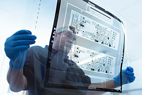
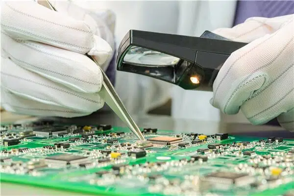
Custom PCB manufacturing is a complex and error-free process. Choosing a custom PCB manufacturer is critical.
PCB fabrication is the process or procedure that transforms a printed circuit design into a body-based on the specifications provided within the design package. Before the fabrication vendor can proceed with the work of building the raw board, there’s a checklist of design details that has to be completed. you ought to choose your PCB fabrication contractor with care, as even small errors can damage the complete board, rendering the tip product useless. Communication between the planning team and makers is critical, especially as manufacturing has moved overseas. This physical manifestation is achieved through the subsequent actions or techniques:
- Imaging desired layout on copper clad laminates
- Etching or removing excess copper from inner layers to reveal traces and pads
- Making the PCB coating stack up by laminating (heating and pressing) board materials at peak temperatures
- Drilling spots for mounting spots, through-hole nails, and vias
- Etching or releasing extra copper from the surface coating(s) to show traces and pads
- Plating pin holes and via holes
- Adding a protective coating to the surface or solder masking
- Silkscreen printing reference and polarity indicators, logos, or other markings on the surface
- Optionally, a finish could also be added to copper areas on the surface
The manufacturing of a printed circuit board is a complex process that begins with a product concept and ends with a totally functional PCB assembly. Along the way a schematic is formed to capture the online connectivity, the physical circuitry is laid get in a PCB design, and electronic components are ordered. After soldering the components onto the board and completing assembly testing and verification, the circuit board is integrated into the total system.
Taking a circuit board from start to end has many intricate details that have got to be completed for fulfillment. One area during this process that doesn’t get the popularity it deserves is that the fabrication of the bare board. The planning of a PCB receives lots of attention thanks to the complex software tools utilized in its creation. Manufacturing will get equally lauded within the satisfaction of completing the ultimate product. But somewhere within the middle of this lies the mysterious process of circuit board fabrication, often unknown outside of the look world.
Custom PCB Printing Steps
Custom PCB Fabrication Process
It might not be helpful to leap directly into fabrication without knowing the relationships and steps between the schematic or idea you’ve got in mind and getting that concept made. Before defining PCB fabrication, it may be helpful to define some other terms and their interrelationships.
Note: PCB manufacturing including PCB fabrication and assembly
- PCB Development
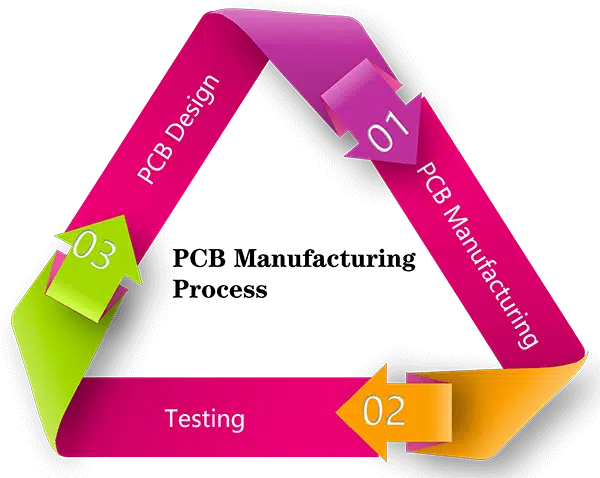
PCB development will be defined because of the process of taking a board design from the planning to the assembly. This generally contains three steps: design, manufacturing, and testing. And for near the best designs, this process is iterative with the target of arriving at the best quality design within the event time allotted.
- PCB Manufacturing
PCB manufacturing is the building of your panel layout. This can be a two-step process that begins with board fabrication and ends with printed circuit board assembly (PCBA).
- PCB Testing
PCB testing, sometimes cited as point out, is that the third stage of PCB development; performed after manufacturing. Testing during development is finished to gauge the board’s ability to perform its intended operational functionality. During this stage, any errors or areas where the planning should be modified to boost performance are identified and another cycle is initiated to include the planning changes.
- PCB Assembly
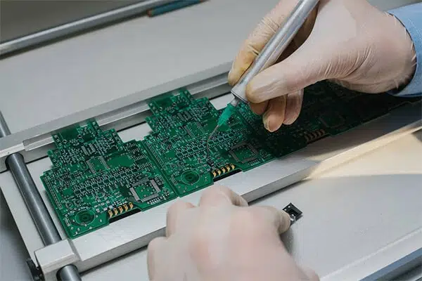
PCB assembly or PCBA is the second step or stage of PCB fabrication within which the board components are mounted to the bare board through a soldering process.
Is it Important to Comprehend the PCB Fabrication Process?
The question can and doubtless should be asked: “Is it important to know the PCB fabrication process?” in the end, PCB fabrication isn't a design activity, it's an outsourced activity that's performed by a contract manufacturer (CM). Although it's true that fabrication isn't a design task, it's tired strict adherence to the specifications that you simply provide to your CM.
In most cases, your CM isn’t aware of your design intent or performance objectives. Therefore, they’d not bear in mind whether you’re making good choices for materials, layout, locations, and kinds trace parameters, or other board factors that are set during fabrication and will impact your PCB’s manufacturability, production yield rate, or performance after deployment, as listed below:
Manufacturability
The manufacturability of your boards relies on a variety of design choices. These include ensuring that adequate clearances exist between surface elements and also the board edge and also the material selected features a sufficiently high coefficient of thermal expansion (CTE) to face up to PCBA, especially for no-lead soldering. Either of those could lead to the lack of your board being built without redesign. Furthermore, if you opt to penalize your designs then that too would force forethought.
Yield rate
Your board is successfully fabricated, while fabrication issues exist. As an example, specifying parameters that stretch the tolerance boundaries of your CM’s equipment may end up in above acceptable numbers of boards that are unusable.
Reliability
Depending upon your board’s intended usage it's classified as consistent with IPC-6011. For rigid PCBs, there are three classification levels that set specific parameters that your board’s construction must meet to realize a specified level of performance reliability. Having your board built to fulfill a lower classification than your application requires will likely lead to the inconsistent operation or premature board failure.
The examples listed above aren’t exhaustive but represent the kinds of problems you will experience if proper fabrication specification decisions aren’t made during design.
Therefore, the solution is an emphatic yes! it’s essential that you just comprehend the PCB fabrication procedure because the design options you create for this phase can reverberate throughout PCB development, production, and even into operation. Your best defense against the categories of problems that will result from not incorporating knowledge of the PCB fabrication process into your design decisions is the utilization of design for manufacturing (DFM) regulations and policies that are established upon the abilities of your CM.
In order to create the simplest use of DFM to protect against unnecessary time delays and extra manufacturing costs, you would like to use a comprehensive and capable PCB design analysis, as JHYPCBA provides. With packages, like the Document Automation Tool, you’ll create multiple detailed views to help your CM during the PCB fabrication process.
Hire JHYPCB for your Custom PCB Fabrication
One of the pioneers in custom printed circuit board fabrication and assembly service, always striving to cope with the ever-advancing pace of technology. The PCB facility at JHYPCB is recently upgraded with the latest equipment to fulfill the wants of the research & development activities of JHYPCB and other organizations.11
Vision:
We deliver custom PCB fabrication and assembly services suiting individual and company requirements. The unmatched fabrication capabilities and customer support make us stand to move into the industry. We guide you thru the steps in the production of a workable output.
The facility includes features such as:
- Computer-Aided Design tools
- Free consulting service for designing and producing the GERBER (.GBR) and drill (.drl) files.
- This leads to upgraded, improved, and rectified printed circuit board production for our clients.
- Experience & trained staffing
- Complex PCB fabrication (Multilayer PCB, Rigid-flex PCB, Flex Circuit, etc.)
- Caring for your individual requirements for printed circuit board fabrication
- No minimum order
- Normal rates
- RF and Microwave Circuits
- Metal Cores
- Plated Edges & Cavities
- UL Certified Laminates
- Bonded Heat Sinks
- Through-hole and Surface Mount Designs
- Gold Fingers
- Buried blind hole PCB and micro vias PCB
- Reverse engineering
Being an industry-leading PCB manufacturer, JHYPCB provides high-quality and quick-turn PCB fabrication and assembly services. Knowing the importance of reducing lead times, we assure the delivery of products and services within the timeframe. Over the years, we’ve developed several capabilities that helped efficiently s fulfill complex PCB fabrication tasks.


FAQs for Custom PCB
The first step in ordering a custom PCB is to export the PCB design files, the Gerber and Drill files, from the EDA software.
Gerber is a standard file format used in the PCB manufacturing industry.
For more information on custom PCB fabrication, click here.
Do you need to order a PCB product with your parameters for your design? Where can I order custom circuit boards?
If you want to order custom PCB products, please refer to the guide below.
1. Criteria for selecting a custom PCB manufacturer
Once you have determined your custom PCB requirements, you can narrow down your selection of PCB manufacturers.
a. Budget
b. PCB material
c. Delivery time
2. Why choose China PCB manufactuer for your custom PCB?
Chinese custom PCB manufacturers are favored by designers and product developers worldwide because of their high quality and low prices.
If you are looking for a reliable custom PCB manufacturer in China, then choosing JHYPCB to provide manufacturing services for your custom PCB will be the right choice.
Advantages of Chinese Custom PCB Manufacturers
- Save Cost
- Quick Turn
- Stable Delivery Time
- High Quality
- Advanced Technology
- Production Standardization
- Complete Manufacturing Capability
- Experienced PCB Experts
If you want to DIY a custom PCB at home, then the build guide below will help you.
1. The basic methods to make a custom PCB
a. Iron on Glossy Paper Method,
b. Circuit by Hand on PCB,
C. Laser Cutting Edge Etching.
2. The Custom PCB fabrication process
STEP 1: Take a printout of the circuit board layout
STEP 2: Cut the Copper Clad Laminate for the Circuit Board
STEP 3: Transfer the PCB Print onto the Copper Plate
STEP 4: Iron the Circuit from the Paper onto the PCB Plate
STEP 5: Etch the Plate
STEP 6: Cleaning, Disposal, and the Final Touches for the Circuit Board
The cost of custom PCB will vary according to different technical needs, such as area sizes, surface finishes, and the number of PCB layers. If you need an inquiry, please send your requirement to sales@pcbjhy.com.
Yes, JHYPCB is a leading PCB manufacturing service provider in China, which can provide you with high-quality, quick-turn custom PCB services with guaranteed delivery.
Absolutely. JHYPCB is an expert in the field of complex multi-layer PCB manufacturing, and can provide you with PCB customization services that meet your needs.
Related Reading
- Custom PCB Fabrication Capabilities
- The Top 11 Custom PCB Manufacturers In the USA
- PCB Fabrication and Assembly Services Manufacturer In China
- What is Prototype PCB?
- What is PCB Panelization and its Methods in PCB Manufacturing?
- Outer Layer Processing of PCB Fabrication Process
- Inner Layer Processing of PCB Fabrication Process