PCB Manufacturing Services
Multilayer PCB Complete Guide & Fabrication Service
The growing popularity of multilayer PCBs
Printed circuit boards (PCBs) are the core of most electronics today, determining basic functions through combinations of components and wiring mechanisms. Most PCBs of the past were relatively simple and limited by manufacturing techniques, while today’s PCBs are way more complex. From advanced flexible options to odd-shaped varieties, PCBs are rather more varied in nowadays’ world of electronics. Of particular popularity, however, are multilayered PCBs.
While PCBs for easy electronics with limited functions are usually composed of one layer, more sophisticated electronics, like computer motherboards, accommodates multiple layers. These are what are called multilayer PCBs. With the increasing complexity of recent electronics, these multilayer PCBs became more widespread than ever before, while manufacturing techniques have enabled them to size down significantly.
Read on to be told more about multilayer PCBs, their uses and advantages within the world of contemporary electronics.
Multilayer PCB Wikipedia
What is Multilayer PCB?
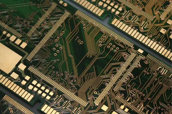
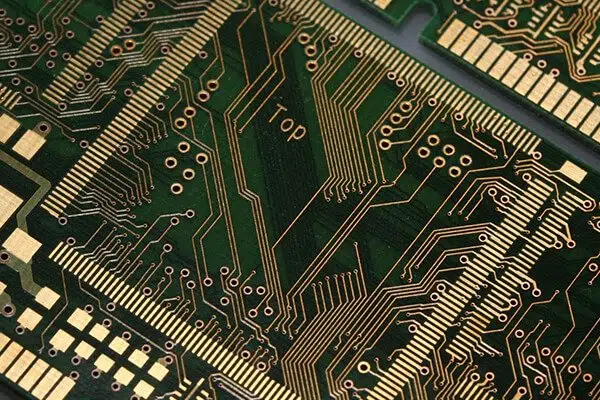
A multilayer PCB is a printed circuit board with three or more copper layers.
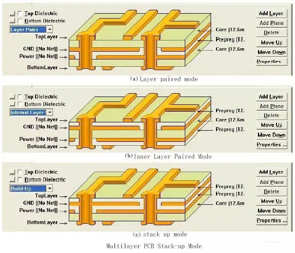
The definition of a multilayer PCB is a PCB that's made with three or more conductive copper foil layers. These appear as several layers of double-sided circuit boards, laminated and glued along with layers of heat-protective insulation between them. The complete construction is arranged in order that two layers are placed on the surface sides of the PCB to attach to the environment. All electrical connections between the layers are achieved with vias like plating through holes, and blind, and buried vias. The application of this method then ends up in the generation of highly complex PCBs of varying sizes.
The multilayer PCB came into being thanks to the evolving changes within the industry. The functions of electronics became progressively more sophisticated over time, requiring more complex PCBs. Unfortunately, PCBs were limited by problems like noise, stray capacitance, and crosstalk, and thus needed to follow certain design constraints. These design considerations made it difficult to induce a satisfactory level of performance from one or perhaps double-sided PCB - thus the multilayer PCB was born.
The layer of Multilayer PCB
Packing the facility of a double-layer PCB into a format that’s a fraction of the scale, multilayer PCBs are getting increasingly popular in electronics. They are available in a very big selection of sizes and thicknesses to accommodate the requirements of their expanding applications, with variants ranging anywhere from four to 12 layers. Layers most frequently are available in even numbers, since odd numbers of layers can cause issues within the circuit like warping, and aren’t any more cost effective to provide. Most applications require between four and eight layers, though applications like mobile devices and smartphones tend to use around twelve layers, and a few professional PCB manufacturers boast the power to provide multilayer printed circuit boards with nearly 100 layers. Multilayer PCBs thereupon many layers are rare to work out, however, as they’re extremely cost-inefficient.
All the layers are compressed to create one Multilayer printed circuit board where all the layers are interconnected via copper-plated holes. All the active and passive electronic components are assembled on top and bottom layers. All the inner stacked layers are meant for routing. Both through-hole electronic components and Surface Mount Components (SMD) are soldered on either side of this sort of PCB. SMD components may be soldered with Surface Mount Technology and other PCBA Tools. A general Multilayer printed circuit board has the following layer stacking:
- Top Layer (Electronic Components)
- Inner Layer-1 (Routing)
- Inner Layer-2 (Routing)
- Inner Layer-3 (Routing)
- Bottom Layer (Electronic Components)
Advantages of Multilayer PCB
From a technical point of view, multilayer PCBs present several advantages in design. These benefits multilayer PCBs present include:
More Powerful
Multilayer PCBs are extremely high-density assemblies, incorporating multiple layers into one PCB. These close-quarters enable boards to be more connective, and their innate electrical properties allow them to attain greater capacity and speed despite their smaller size.
Lightweight Construction
With smaller PCBs comes less weight, especially because the multiple connectors required to interlink separate single and double-layered PCBs are eliminated in favor of a multilayered design. This, again, is useful for contemporary electronics, which are geared more toward mobility.
Increased Durability
Multilayer PCBs tend to be durable by their nature. Not only do these multilayer PCBs need to withstand their own weight, but they need to even be able to handle the warmth and pressure want to bind them together. On top of those factors, multilayer PCBs use multiple layers of insulation between circuit layers, binding it all at once with a prepreg bonding agent and protective materials.
Small Size
One of the foremost prominent and lauded benefits of using multilayer PCBs lies in their size. Due to their layered design, multilayer PCBs are inherently smaller than other PCBs with similar functionality. This presents a serious benefit to modern electronics because the current trend is functioning toward smaller, more compact yet more powerful gadgets like smartphones, laptops, tablets, and wearables.
Enhanced Flexibility
Though this doesn’t apply to all or any multilayer PCB assemblies, some do use flexible construction techniques, leading to a versatile multilayer PCB. This is a highly desirable trait for applications where mild bending and flexing may occur on a semi-regular basis. Again, this doesn’t apply to all or any multilayer PCBs, and therefore the more layers incorporated into a versatile PCB, the less flexible the PCB becomes.
High-Quality
Thanks to the quantity of labor and planning that has to come with the creation of multilayer PCBs, these kinds of PCBs tend to be better in quality than single and double-layer PCBs. They also tend to be more reliable as a result.
Single Connection Point
Multilayer PCBs are designed to figure as a singular unit, instead of in tandem with other PCB components. As a result, they need one connection point, instead of the multiple connection points required to use multiple single-layer PCBs. This proves to be a benefit in electronic product design additionally since they only must include one connection point within the final product. This can be particularly beneficial for tiny electronics and gadgets designed to attenuate size and weight.
These benefits make multilayer PCBs highly useful in an exceeding form of applications, particularly mobile devices and high-functioning electronics. In turn, with such a large number of industries turning to mobile solutions, multilayer PCBs are finding an area in an increasing number of industry-specific applications.
Disadvantages of Multilayer PCB
The benefits of multilayer PCBs are numerous, making them applicable to a good form of advanced technologies. However, these sorts of PCBs aren’t appropriate for all applications. In fact, several drawbacks can outweigh multilayer PCB advantages, especially for electronics of lower cost and complexity. These disadvantages include the following:
- Higher Cost
Multilayer PCBs are significantly costlier than single- and double-layer PCBs at every stage of the manufacturing process. They’re difficult to style, taking an in-depth amount of your time to figure out any potential problems. They also require a highly complex manufacturing process to supply, which takes a good deal of your time and labor on the part of assembly personnel. Additionally, because of the character of those PCBs, any mistake within the manufacturing or assembly process is prohibitively difficult to remodel, leading to either additional labor costs or scrap material expenses. On top of it all, the equipment accustomed produce multilayer PCBs is kind of expensive because it’s still a comparatively new technology. For all those reasons, unless small size is an absolute necessity for the appliance, cheaper alternatives are also a stronger choice overall.
- Complicated Production
Multilayer PCBs are harder to provide, requiring way more design time and careful manufacturing techniques than other PCB types. This can be because even small flaws within the PCB’s design or manufacture could render it useless.
- Limited Availability
One of the biggest issues of multilayer PCBs is the expenses of the machinery needed to supply them. Not all PCB manufacturers have the funds or the requirement for this machinery, so not all PCB manufacturers carry it. This limits the amount of PCB manufacturers available to supply multilayer PCBs for clients. Thus, it is best to carefully inquire about a PCB manufacturer’s capability in terms of multilayer PCBs before deciding on your contract manufacturer.
- Skilled Designer Required
As previously discussed, multilayer PCBs require extensive design beforehand. Without previous experience, this may be problematic. Multilayer boards require interconnection between layers, but must simultaneously mitigate crosstalk and impedance issues. one problem within the design may result from a non-functioning board.
- Production Time
With increased complexity comes more manufacturing requirements. This plays into a key issue with multilayer PCBs’ turnover each board requires a big amount of your time to provide, leading to more labor costs. Additionally, it possibly results in longer periods between when an order is placed and when the merchandise is received, which may be a controversy in some circumstances.
However, these issues don’t diminish from the utility of multilayer PCBs. While they have a tendency to cost quite one layer PCB, a multilayer PCB claims many advantages over this sort of printed circuit board.
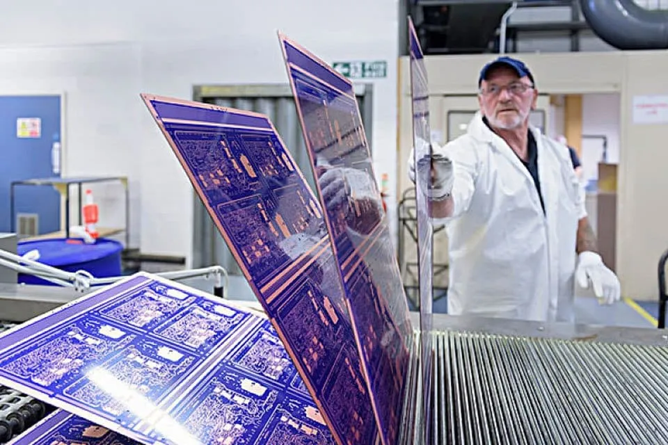
Multilayer PCB Manufacturing Process
Multilayer PCB manufacturing process needs special precaution as there are more chances of cross-connections, overlaps, tracing in copper areas, etc. the full process has to be worn out in an ESD-Safe and Cleanroom environment. Special manufacturing setup and equipment are needed for the 8+ layer PCB manufacturing process.
Following are the steps involved in Multilayer PCB Manufacturing Process:
- The process starts with designing Layout of the PCB using any PCB designing software / CAD Tool (Proteus, Eagle, OrCAD).
- Next step is to create the Inner Layer Core. Laminate of desired thickness is treated with copper foil, dry film resists and UV light to create the inner layer core.
- Next step is lamination. This process include: Inner layer core, prepeg sheets and copper foil sheets. The sheets of fabric are staked on one another and holes are wont to align them as they’re stacked up.
- For a 4 layer board, Staking of layers is as follows: Bottom Layer of Copper Foil – Prepeg Sheets – The Inner Layer Core – More Prepeg Sheets – Finally Copper Foil Sheet on Top.
- Next step is to use pressure, heat and vacuum employing a heated mechanical press. Vacuum is vital to create sure there’s no air trapped between the layers. This process ends over 2 hours betting on the number of layers.
- Once cured, resins from the prepegs join the sheets, core, and foil together forming a multilayer PCB.
Multilayer PCB Fabrication Process
Uses of Multilayer PCB
Multilayer printed circuit Boards offer more flexibility and increased circuit density with reduces size. This is often why many electronic companies within the world use these boards in several electronic devices and gadgets:
- Computers and Laptops
- Telecommunications Equipment – portable, Tablets and other Hand Help Devices
- File server and Data storage
- Signal transmission, movable repeaters, GPS
- Satellite
- Medical Equipment: Testing, X-Ray, cardiac monitor, CAT Scan
- Industrial Equipment
- Atomic and Nuclear Systems
- Military and Defense Equipment
- Automotive
- Aerospace
- Anywhere, where complex Circuitry is required.
Why Are Multilayer PCBs So Widely Used?
The specific applications listed above represent only a fraction of multilayer PCBs applied throughout the industry. But why are they used so widely? Much of the favoritism toward multilayer PCBs lies in industry trends. With electronics progressing ever toward miniaturization yet multi-functional options, the inner components of these electronics must follow the identical trend. While single and double-sided PCBs have proven limited in their ability to balance size and functionality, multilayer PCBs provide a comprehensive solution.
While there are several drawbacks to using multilayer PCBs over single and double-layer options, like increased costs, design times and production inputs, these costs are getting more accepted in today’s world. Functionality is basically favored over cost, and folks are willing to pay more for prime capacity electronics. Additionally, because the technology becomes increasingly mainstream, production techniques and machinery will eventually settle down expensive, especially as new techniques arrive within the industry. With those irreversible trends and continuing progress of technology, many expect to determine multilayer PCBs become even more abundant within the future.
FAQs
The difference between single-sided PCB, double-sided PCB, and multi-layer PCB lies in the number of inner layers.
Single-sided and double-sided circuit boards have no inner layers, single-sided PCBs have only one side with circuits, and only one side is used to install electronic components; double-sided PCBs have circuits on both sides, and electronic components can be installed. Multilayer PCBs have printed circuit boards with three or more inner layers, enabling more complex designs and functions.
The inner layers (Internal Plane) of a multilayer PCB are generally connected to ground and power and become the power and ground layers. The inner layer also has the function of electrical connection and is also the actual copper layer, but the inner layer is not wired and is composed of a whole piece of copper.
The mechanical layer defines the appearance of the entire multilayer PCB board. It is generally used to set the overall dimensions, data marks, alignment marks, assembly instructions, and other mechanical information of the circuit board.
The Silkscreen layer is mainly used to place printing information, such as outlines and labels of components, various annotations, characters, etc. Top overlay and Bottom Overlay are provided in Protel 99 SE.
Multilayer PCB is mainly laminated by three materials: inner layer core, prepreg (woven glass cloth with epoxy resin), and Cu foil.
Yes, we provide multi-layer PCB assembly services. See details here.
Yes, we are a leading PCB manufacturer in China, capable of handling complex and up to 64 layers of multi-layer PCB manufacturing services.