Soldering is a huge part of the printed circuit board design process. The sole reliable thanks to getting your circuits to stay to your board and stay there by soldering them on. Without soldering, there are not any printed circuit boards. Wave soldering could be a technique used for big-scale PCB assembly for fast soldering of boards that use either or both SMDs and led components. Wave soldering is much less widely employed in PCB assembly than it absolutely was in previous years. Despite this, wave soldering remains a process that may be used effectively in a number of areas, especially when the PCB assembly uses a combination of leaded and SMT components.
Wave soldering is employed within the creation of printed circuit boards. It’s often used as some way to make boards in mass quantities during a touch of your time. Additionally, to being fast, wave soldering is additionally efficient and stable thanks to applying components to a printed circuit board. For those that are searching for soldering processes that are quick and efficient, it’s hard to seek out one better than the wave soldering process. Let’s talk more about what wave soldering is, what it’s best for, and therefore the complications that you simply may encounter.
What is Wave Soldering?
One of the foremost common kinds of bulk soldering is wave soldering. Wave soldering may be quick and effective thanks to attaching different electrical parts to a PCB, a printed circuit board. This can be often finished with tin alloys. Wave soldering may be a bulk soldering process that permits one to manufacture many circuit boards in a very short amount of your time. It works by passing each board over a pan of molten solder. A pump within the pan creates a “wave” of solder that washes over the board, soldering the components to the board. The PCB then receives a water spray or air blowing to soundly turn and fix the parts in situ.
Proper temperatures are important during the wave soldering process. Failing to sufficient control for temperature can put mechanical stress on the board, which might cause cracks and loss of conductivity. Insufficient preheating can cause cavities, which might compromise both board strength and conductivity. The incorrect solder temperature may result in failure to get the right solder thickness, which could make the board more prone to stress.
Wave soldering Machine
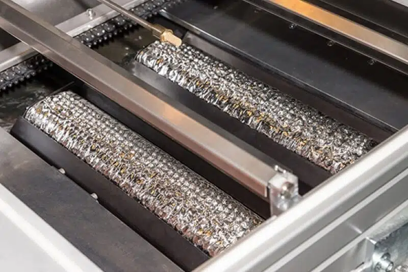
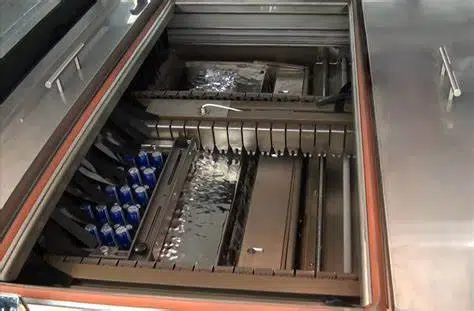
The wave soldering device consists of a heated tank of solder. This is often maintained at the specified temperature for the soldering process. Within the tank, a wave of solder is about up and also the printed circuit boards are missed out this so the underside of the board just contacts the solder wave. Care must be taken in adjusting the peak of the wave so it doesn’t flow over the highest side of the board which might cause the solder to enter places where it’s not required. The boards are held firmly in situ on a conveyor using metal fingers. These are typically products of titanium because it’s ready to withstand the temperatures and it’s not laid low with the solder.
Preparation
In order that an electronics printed circuit board is also successfully processing employing a wave soldering machine, it’s necessary that it’s designed and made in the correct manner.
- Solder Resist Layer
The primary is standard practice when designing boards nowadays. A solder resist or solder mask layer is included within the printed circuit board design, and this adds a layer of “varnish” like material to the board to which the solder won’t adhere. This solder resist is most typically green in color.
- Pad Spacing
The second main precaution is to make sure that there’s sufficient spacing between the solder pads requiring soldering. If they’re too close then there’s the likelihood that the solder may bridge the 2 pads causing a brief circuit.
In view of the way that wave soldering works, where the solder wave is caused by the solder flowing out of the reservoir tank, and also the board passes over it, the spacing needs are conditional upon the tendency of the board comparative to the solder flow. Pads that are spaced apart within the direction of the solder flow should have a greater spacing than those that are spaced at right angles to the solder flow. This can be because it’s much easier for solder bridges to occur within the direction of the solder flow.
Fluxing
To make sure that the places to be soldered are neat and clean and also free from oxidation, etc., flux is required. Flux is used to the side of the board to be soldered, i.e., the underside. Careful control of the quantities of flux is needed. Deficient flux and there’s a high risk of poor joints, and an excessive amount of flux and there’ll be residual flux on the board. While this doesn’t look good cosmetically, there’s also the danger of long-run degradation thanks to the acidic nature of the flux. There are two major techniques of applying the flux:
- Spray Flux
A fine mist of flux is sprayed onto the underside of the board that’s to be soldered. Some systems may even use a compressed gas jet to get rid of the surplus flux.
- Foam Flux
The electronic printed circuit board omitted a cascading head of flux foam. This can be generated by employing a tank of flux into which a plastic cylinder with tiny holes is immersed. The plastic cylinder is roofed with a metal chimney and the air is forced through the cylinder. This causes flux foam to stand up the chimney.
Preheat
The wave soldering process exposes the electronic printed circuit boards to considerable levels of warmth, far greater than those it’d be subjected to if it were to be manually soldered. This thermal shock would produce a considerably increased level of failure if it weren’t addressed. To beat this the board is preheated so it is steadily observed to the specified temperature steadily in order that any thermal shock is minimized.
The prewarming area generally uses warm air heaters that blow warm air onto the boards as they pass towards the wave soldering machine. On some occasions, particularly if the board is densely populated, infra-red heaters could also be used still. This ensures that each board is evenly heated and no shadow areas are present.
While the pre-heating is required to forestall the thermal shock that the wave soldering machine would generate, the heating is additionally necessary to activate the flux. This flux is required to make sure that the areas to be soldered are clean and can take the solder.
Wave Soldering Process
In this step, it’s time actually to use the solder to the printed circuit. On wave soldering machines, the solder is truly a paste until it begins to heat up. Once it heats up, it acts as a wave or waterfall that the card will pass under. The solder utilized in wave soldering is usually a mixture of lead, tin, and antimony. For a lead-free alternative, more and more production skills are using tin silver copper or tin copper nickel alloy mixtures.
Cooling The Board
Although cooling is the final step within the wave soldering process, it’s still essential. Allowing your printed circuit to cool down slowly can make sure that your components are properly sealed and that your board is in excellent condition. Forcing your board to cool down too quickly may result in damage. Even too slowly are often a recipe for disaster.
The ideal thanks to cool your freshly soldered board is by employing a spray bottle with cool water or cool air. you would like to chill your circuit card at a gradual rate, and using these methods will allow you to manage the cooling process.
The Difference Between Wave Soldering and Reflow Soldering
- Wave soldering could be a solder that forms a solder peak to solder components. Reflow soldering is a warm temperature of hot air to create a reflowed molten solder to solder components.
- During reflow soldering, there’s solder on the PCB before the furnace, and only the coated solder paste is melted and welded after soldering. During wave soldering, there’s no solder on the PCB before the furnace, and therefore the solder wave generated by the welder coats the solder on the pads to be soldered.
- Reflow soldering is suitable for SMD electronic components, and wave soldering is suitable for pin electronic components.
Conclusion
For those functioning on bulk printed circuit boards, wave soldering is genuinely the most effective choice to maximize outcomes and keep costs as low as they’ll be. Wave soldering uses four different steps to make the wave soldering process. Wave soldering uses a mix of flux, heat, and solder to assist combine electrical components through both surface mounting additionally as through-hole mounting. The whole wave soldering process is completed through a machine that cuts down on mess but includes a massive increase in terms of space used.