PCB Soldering Techniques
The process used to attach components to a PCB is soldering. There are multiple soldering methods used to bond components to a bare PCB. Your PCB assembler will determine the appropriate soldering method and process for your particular board, so you won’t need to specify this yourself. However, it’s important to understand how automated soldering processes work and the preparation required to ensure successful assembly.
Preparing for PCB Soldering
As was mentioned above and in earlier lessons, there are two sets of data needed in the PCB assembly process:
- A paste mask stencil, which is used to apply solder paste
- A pick-and-place file which tells automated machinery where to place components on the bare board
The paste mask data in your fabrication files will be used to create a paste mask stencil, which will be used with SMD components.
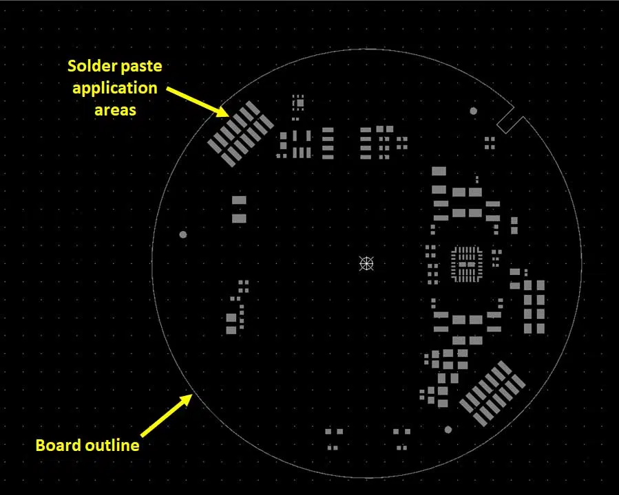
This image shows a paste mask layer as defined in a Gerber file.
Two important materials used in soldering are solder paste and solder flux. A solder paste is coated over the exposed SMD pads with the paste mask stencil, and the paste will harden into a solid joint during soldering. For through-hole components used in wave soldering, solder flux must be applied to the bare board, usually with a spray. Once applied, the flux will break down oxides on the surface of exposed conductors, and it will cause molten solder to adhere to the coated conductor. Solder paste includes a solder flux, so flux is unnecessary when using a solder paste in an SMD process.
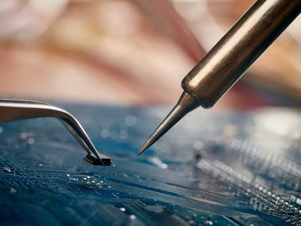
Hand Soldering
The most basic method of soldering is manual soldering or hand soldering. Assemblers don’t normally use hand soldering except for special components that can’t fit into a standard pick-and-place machine. Hand soldering works just like it sounds; components are manually placed and soldered using a soldering iron and thin-gauge solder wire. Some examples of components that might be hand soldered due to their awkward shape or pad arrangement include specialty connectors or edge connectors, castellated modules, and some surface-mount sensors.

Hand Soldering - Manual Soldering
Hand soldering is basically obsolete in modern PCB assembly facilities, and it is only used when necessary. There are several reasons for this, but the three major reasons are throughput, consistency, and cost. Hand soldering is a slow process, and the solder joint’s quality depends on the assembler’s skill. In addition, not all components can be easily hand soldered. An example would be an SMD component with the pads on the bottom of the package, which can’t be accessed with a soldering iron or wire. Because of these drawbacks, automated processes are preferred in PCB assembly.
Wave Soldering
Wave soldering is used for soldering through-hole components in bulk. In this process, the entire board is populated with components and passed through a bath of molten solder. The solder then coats the exposed (fluxed) through-hole landing pads, and the solder eventually cools to form a solid joint. During this process, the molten solder bath is pumped from beneath so that it forms a “wave” that washes over the PCB, hence the name of this process.
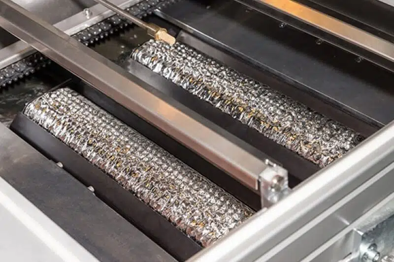
Wave Soldering at Work
Reflow Soldering
In reflow soldering, solder paste is applied to SMD pads on the bare PCB and the board is populated with components using a pick-and-place machine. The board is then conveyed into an oven held at high temperature (approximately 200-250 °C). During soldering, the oven temperature is slowly increased up to its highest value over time to ensure proper soldering and prevent component damage. Once the solder paste heats up to high temperature, it becomes molten and begins to flow onto exposed conductors, where it wets and adheres. As the board moves out of the oven, it begins to cool and the solder solidifies, forming a hard joint.
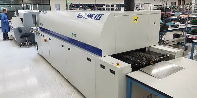
Reflow Soldering
Selective Soldering
Selective soldering is effectively a mix of automated hand soldering and wave soldering for through-hole components. This process is often used in PCBs that are assembled with a mix of reflowed SMD components and through-hole components. Another instance where selective soldering is used is when the soldered component might be sensitive to the high temperatures in a reflow oven or wave soldering bath. The SMD components or temperature-insensitive components are processed first, followed by application of selective soldering.
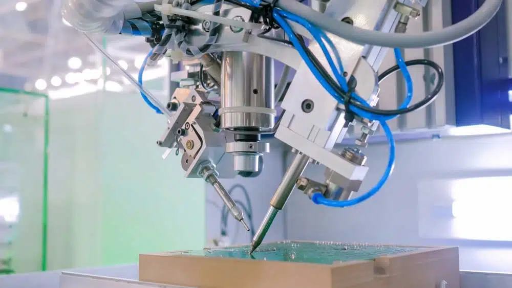
Selective Soldering
Selective soldering can be used for targeted soldering of through-hole components with an automated system.
Selective soldering proceeds in three steps:
- Flux or solder paste is applied to solder points
- The assembly and apparatus are pre-heated to the required temperature
- The solder nozzle is scanned across the board and the target areas are soldered
During the 3rd step, molten solder is ejected from the solder in a manner similar to a wave process. This molten solder is confined in the location near the solder nozzle, so it will only create a solder joint at that particular component.