Overview
Automated printed circuit board assembly equipment often has trouble working with smaller boards, leading to more frequent defects during the assembly process. to attenuate these defects and improve the throughput of the manufacturing process, many companies use a process called panelization, leading to a PCB panel. Board uniformity is the primary concern in any circuit board manufacturing project. The boards that are non-uniform are discarded because they’re ineffectual to satisfy the requirements of an intended application. The assembly process for large and little remains identical, some changes are made during small PCB production to keep up their quality.
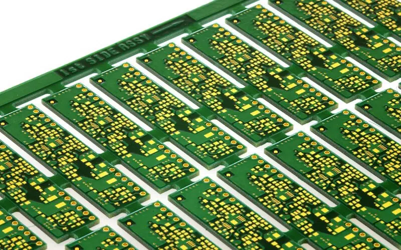
PCB panelization is performed during the assembly of small circuit boards to make sure uniformity. during this method, various small-sized circuit boards are pooled together to create an outsized panel. This helps manufacturers assemble multiple small PCBs simultaneously. Thus, manufacturers can improve their productivity, moreover, as ensure uniformity, and quality of circuit boards. The panelization technique is additionally referred to as an array format because multiple boards are kept together. PCB panelization permits creators to obtain high-quality boards in big volumes. This post discusses everything you wish to grasp about PCB panelization.
What is a PCB Panel?
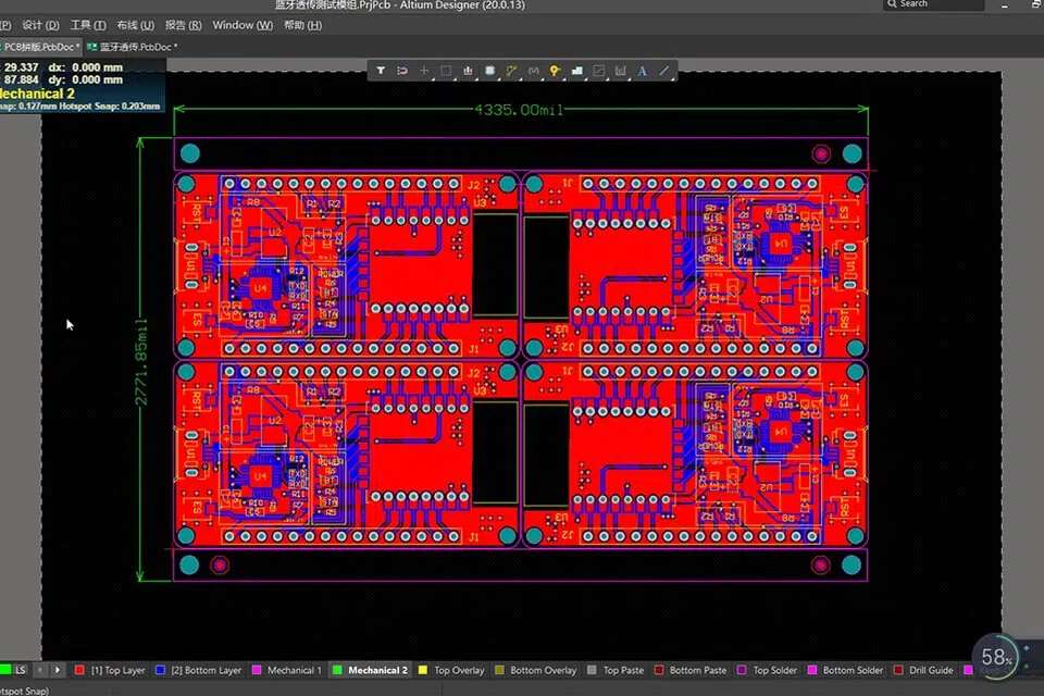
A PCB panel, also called a PCB array, could be a single board consisting of multiple individual boards. Once manufactured, the panel is then smashed apart or depanelized, into the single PCBs during the breakout procedure. The advantage of the printed circuit board panelization process may be a decrease in defects as automated assembly machines tend to encounter fewer problems during the assembly process. Additionally, panelization also reduces cost by improving throughput.
Successful PCB panelization requires multiple design specifications to figure properly, including considerations surrounding panelization methods. We’ll detail these PCB panel methods and their specific requirements more thoroughly during this set of panelization guidelines.
PCB Panelization Methods
There are many panelization methods exist, each with its own advantages and disadvantages. The look of the boards on the panel and therefore the panel itself will often play an outsized role in which panelization method most closely fits the application. The foremost notable of those factors include:
Design
The planning of the board plays the most important part in determining the foremost appropriate panelization method. The number of clearances between components and therefore the fringe of the board may ensure methods much less suitable than others, as does the presence of edge-hanging components.
Components
The categories of components used on the board are even as important as their placement. Particularly sensitive components and connectors may play an element within the most appropriate breakout and panelization method.
Materials
The materials employed in a PCB may limit which kind of panelization method is most appropriate, as some materials are more vulnerable to splintering during the breakout process. Board thickness is additionally an element, as particularly thin boards could also be more likely to interrupt during assembly, and thick boards may prove more problematic during the breakout process.
These factors limit the alternatives available to anyone application. In fact, many assembly companies may use a mixture of methods on anyone project to make sure the structural integrity of the array while still mitigating issues during the breakout process.
There are three methods of panelization in use today, though only two are commonly practiced. They are:
1. V-Score Panelization
This usual technique of panelization discrete single PCBs with V-shaped grooves. These grooves remove approximately a 3rd of the board’s thickness from the highest and bottom of the board with an angled blade. A machine is usually wont to finish the breakout process, considering the remaining third of the board between the grooves is surprisingly strong, and hand-breaking can put stress on the PCB and surrounding components.
2. Tab Routing Panelization
With this method, PCBs are pre-cut from the array and held in situ on the board with perforated tabs. Three to 5 holes are often utilized in these perforation patterns. This method is commonly beneficial for its ability to support designs with edge-hanging components. It may be broken by hand rather than with tools.
In this method, space is left between the traces, perforated tabs, and surface-mounted components. Tab route panelization is performed on PCBs of identical or differing designs. This method isn't viable for heavy-weight components like large relays or transformers. During tab separation, small laminate nubs may remain, which are usually sanded to attain smooth PCB edges.
3. Solid Tab Panelization
Arrays will be designed with solid tabs between each board, improving overall strength. However, the depaneling method for this sort of PCB panel requires either a depaneling router, a laser-cutting machine, or a hook-shaped blade tool. The router may result in dust and vibration, while the laser-cutter is extremely expensive and ineffective on boards over 1mm thick. The hook-bladed option is a smaller amount expensive but inefficient and susceptible to blade rotation. This method tends to be less common than the opposite two.
4. V-groove Panelization
In this method, a printed circuit board is cut in 1/3rd thickness from top and bottom employing a 30–45-degree blade in a circular shape. The remaining board is depaneled employing a machine. V-groove panelization is right if there are not any overhanging components. This method is right for scoring rectangular and square-shaped PCBs. If your PCBs don’t have irregular or curved edges, then this method isn't ideal.
Conclusion
V-Score and Tab Routing are the popular panelization methods for many applications. the foremost important thing for PCB designers is knowing which of the 2 methods is best for their application. The following step is to style their array for maximal strength and breakout success. We like better the V-groove panelization technique, when is possible, for its expertise and reduction in surface stress. Depaneling machines for this sort of array also are relatively inexpensive and cost-efficient. Even better, they’re portable and need minimal maintenance. Though the strategy tends to end in rougher board edges, this can be rarely a priority for applications where V-groove panelization is employed.