The PCB Fabrication Process
Now that your multilayer PCB board design is completed, the board has passed a design review, and all of your files are prepared, it’s time to move it into manufacturing. The first half of the manufacturing process is fabrication, where the bare board is produced and inspected before being sent off to assembly. The PCB fabrication process first begins by converting manufacturing files into tooling. Then, the board passes through a series of chemical and mechanical processing steps to build up the PCB stackup with its printed elements. Finally, the fabricated board will be inspected using a series of tests to ensure it has the required electrical behavior.
In this section, we’ll focus on the fabrication process used for rigid PCBs. Flex and rigid-flex PCBs, as well as HDI PCBs, have their own specialized fabrication processes. We’ll also focus on standard processing with vias, meaning through-hole vias no smaller than 6 mils in diameter. Narrower vias may require HDI fabrication techniques, which are best covered in a dedicated design course. The techniques covered here are standard for the vast majority of PCBs that are manufactured today and can cover advanced designs operating at very high speeds and frequencies.
Standard PCB Fabrication Steps
PCB fabrication involves producing individual layers in the PCB in succession, followed by pressing these into the stackup and drilling any holes and routes into the surface of the board. After these processes, solder mask is applied and a plating process is used to plate up exposed through-holes and form vias. Once the PCB is fully plated, a surface finish is applied to the exposed conductors. After final cleaning and inspection, the board is ready for assembly.
Now, we want to explore each of these portions of the fabrication process. PCB fabrication starts by first forming the inner layers of the PCB and then building the stackup.
Inner Layer Processing
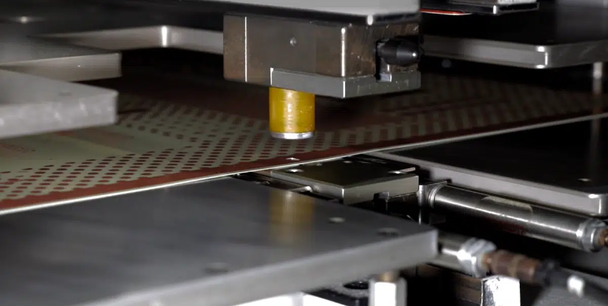
Fabrication begins by etching features into each layer of the PCB. Each layer of copper-clad core or prepreg is fabricated individually with a photoimaging process. This process is a lithography process, where a stencil is used to define areas of copper that will be stripped from each layer. An overview of the process is shown below.
Step 1: Stencil Creation
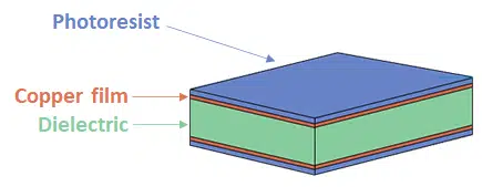
Before any fabrication steps are performed, the Gerber files (or ODB++/IPC-2581 files) are used to create stencils that will be used to form copper features on the inner PCB layers. Each layer has its own stencil that contains all the copper features to be formed on a layer in the PCB. The remaining fabrication steps are performed with copper-clad laminates (core material), which is covered on both sides with copper. The copper in each layer will be etched during the remaining fabrication steps.
Step 2: Photoresist Coating
PCB fabrication begins by taking a copper-clad PCB laminate and preparing to etch the un-used copper away from the top and bottom sides. To do this, a photoresist material is used. This material is a liquid polymer that will harden when exposed to UV light. The photoresist is first coated over both sides of the entire panel.
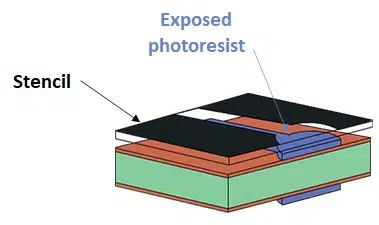
Step 3: Photoresist Exposure and Removal
Once the panel is coated with photoresist, the photoresist is exposed to UV light through one of the stencils. The exposed region of photoresist will match the copper features that were defined in the stencil in Step 1. Once the exposed photoresist hardens, the stencil is removed and the remaining photoresist is removed with a solvent.
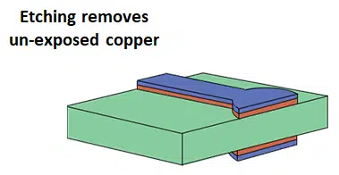
Step 4: Copper Etching
The copper etching step involves immersing the panel in a solution of ferric chloride [FeCl3], ammonium persulphate [(NH4)2S2O8], sodium persulfate [Na2S2O8], or cupric chloride [CuCl2]. During the copper etching step, the exposed photoresist will protect the covered copper from the etchant solution. After etching has completed, only the protected copper and its overlaid photoresist will remain on the panel.
Step 5: Photoresist Removal
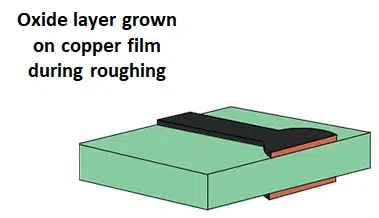
After the un-needed copper is etched away from the panel, the remaining photoresist is removed with a solvent. This leaves behind etched copper on the exposed dielectric material.

Step 6: Roughening
The last step that is needed to prepare for lamination is copper roughening. Copper films that are found on inner layers of PCBs are typically so smooth that the resin layer will be unable to bond to the film. Therefore, the copper is intentionally roughened in order to provide a surface for the next layer to “grab” during lamination. The roughening process leaves behind a black oxide film on the exposed copper. At this point, the boards will be ready for multilayer lamination.
Step 7: Inner Layer Inspection
After inner layer processing is completed for each layer, the layers are inspected using automated optical inspection (AOI) equipment. AOI involves scanning the copper pattern on each side of the detail to ensure there are no defects such as shorts, opens or stray bits of copper left behind. If a panel is identified to have defects, it can be scrapped and a new layer can be fabricated in its place.
Some additional steps are needed before moving to the next stage of the process. In the past, alignment holes were punched in the panel for each layer pair so that the panels could be aligned in the multilayer lamination step. Today, optical target systems can be used to align panels, which is much more accurate and is needed to reach very small clearances used in some PCBs.
Step 8: Multilayer Lamination
The multilayer lamination process is where each of the layers in the PCB will be pressed into a finished PCB stackup. The idea behind this process is simple: the board layers are stacked on top of each other and they are compressed at high temperature until the layers bond together.
If you recall the structure of PCB laminate materials, you should remember that these materials are primarily resin-based materials. During the lamination process, the layers are held at high temperature (approximately 350 F) and pressure (approximately 300-400 psi) so that the resin in each layer can melt and flow at the interface between layers. As the stack is allowed to cool, the mix materials will form a strong bond as the resin solidifies, leaving a laminated stack of layers that is ready for the next steps in the manufacturing process.