After you’ve created your order with a PCB fabrication house and sent in your fabrication files, the PCB fabricator will perform a DFM(Design For Manufacturing) evaluation to ensure the board can reliably pass through their process. PCB fabricators use specialized software to quickly scan Gerbers for any features that could produce a fabrication defect leading to a scrapped board. Once the board is scanned and examined, the fabricator usually provides a report that shows.
Many of the points that are examined during a DFM evaluation relate to feature sizes and clearances. While this might sound simple, these aspects of your layout are critical in DFM. If clearances are too close or features like pads and traces are too small, it’s possible there will be an unintended short circuit or open circuit in the board, and the board would need to be scrapped. This occurs because the etching and plating processes used to fabricate copper features are imperfect and only reliable down to certain size limits.
The image below shows an example of a fabricator’s DFM analysis results. Your fabricator may send you a similar report showing examples of DFM violations.
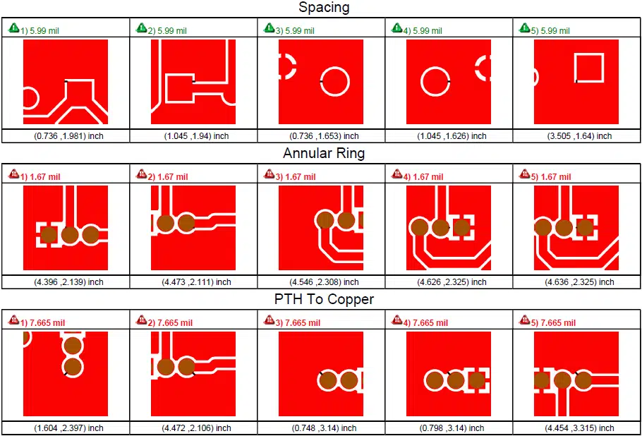
In the above image, there are two principle sets of defects:
- Pad sizes in the design are too small. This means the leftover pads attached to any vias are too small to pass IPC reliability standards, which will need to be increased.
- The clearance between copper polygons, planes, and ground pour is too small. The design rule governing copper clearances should be changed, and the copper regions should be reconstructed.
Your fabricator will tell you exactly what needs to change in the design to ensure the board can be fabricated reliably.
In the past, making these changes would be time-consuming, but today’s ECAD software can help you quickly make these corrections. Altium Designer and other CAD tools have useful features that will automatically check for remaining clearance violations after you modify your design rules. You can quickly correct the violations before sending the design back for PCB fabrication.
There are other aspects that a fabricator will need to check to ensure they can fabricate the design. It’s often the case that simple mistakes will prevent a board from being producible. Here are some of the most common problems:
- Tight clearances, as shown in the example above
- Missing teardrops in high-reliability designs
- Annular rings that are too small
- Through holes that are too small or too large
- Stackup thickness or layer thickness that is non-standard
- Antipads that are too small due to clearance settings
- Disconnected planes/polygons and vias
- Thin solder mask slivers between SMD pads
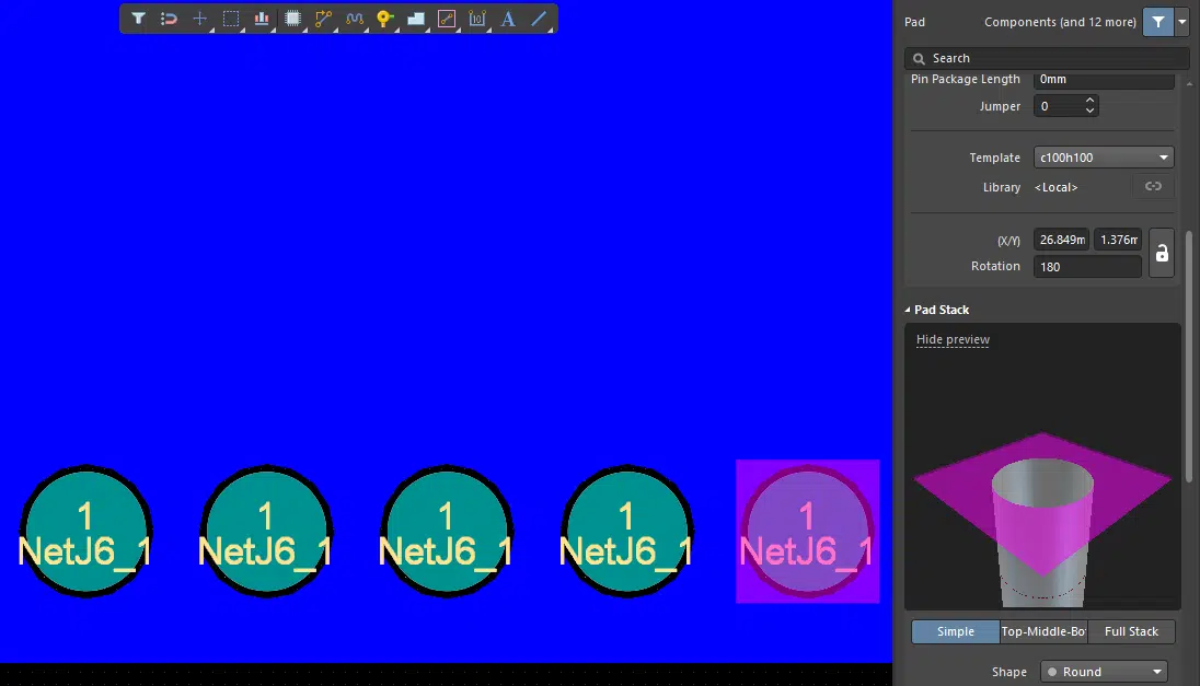
This image shows a simple example of a net disconnection between a via and a polygon. This disconnection was not flagged by Altium Designer, but it will get flagged during a DFM check.